Skip to content
Back to Modules
Part IA Michaelmas Term

Digital Electronics

Digital-Electronics Logic-Gates Boolean-Algebra Karnaugh-Maps Sequential-Logic Flip-Flops FSM State-Machines CMOS Transistors Processor-Architecture Hazards Adders Multiplexers Memory Electronics Part IA Michaelmas Term Paper 2
  • Combinational Logic Foundations

    Abstraction levels in digital electronics, logic variables and gates (AND, OR, NOT, XOR, NAND, NOR), Boolean algebra, DeMorgan's theorem, and the consensus theorem

    • Introduction and Abstraction

      What is Digital Electronics?

      Digital electronics is the branch of electronics concerned with circuits that process binary signals: signals that take one of two distinct voltage levels representing logical 0 and logical 1. The course covers how to design, build, and test systems built from logic gates, combinational circuits, sequential circuits (with memory), and ultimately simple processors.

      Unlike analogue circuits, where signals vary continuously, digital circuits are inherently robust: because only two voltage levels are distinguished, small amounts of electrical noise do not corrupt the signal. This noise immunity is one reason digital systems dominate modern computing.

      The Six Levels of Abstraction

      Modern digital systems, such as microprocessors, contain millions of transistors. Designing such a system by modelling the behaviour of individual electrons is not feasible. Instead we manage complexity through abstraction: hiding details that are not relevant at a given level of analysis.

      For an electronic computing system, eight levels of abstraction are commonly identified, from the physical to the application:

      LevelDescriptionExamples
      PhysicsElectrons and fieldsQuantum mechanics, Maxwell’s equations
      DevicesIndividual transistorsWell-defined current-voltage characteristics between terminals
      Digital CircuitsGates assembled from transistorsAND, NOT, NAND gates
      Logic ElementsComplex structures from digital circuitsAdders, memories, multiplexers
      MicroarchitectureData paths and controllersCombines logic elements to execute instructions defined by the architecture
      ArchitectureInstruction set and registersIntel IA-32 defined by its instructions and register set
      Operating SystemsResource managementDevice drivers, memory management, file systems
      Application SoftwarePrograms that use OS facilitiesWeb browsers, word processors, games

      In this course we are primarily concerned with the shaded middle levels: Digital Circuits, Logic Elements, and part of Microarchitecture. The abstraction principle means that when working at the gate level, we treat each gate as a black box with a known logical function; we do not need to understand the transistor-level physics inside, though knowing something about the levels above and below helps: a device designer should understand the circuits in which the device will be used, and code cannot be optimised without understanding the architecture for which it is written.

      Managing Complexity

      Abstraction works because each level provides a well-defined interface to the level above. At the gate level:

      • A NOT gate always inverts its input. We do not care how many transistors implement it or what voltages represent a 1.
      • An AND gate always produces TRUE only when all inputs are TRUE.

      This layered thinking means we can browse the web (application software level) without any regard for quantum theory or the organisation of memory in the computer. However, awareness of adjacent levels is valuable: you cannot write efficient code without understanding the architecture; you cannot design good gates without understanding the circuits they will form.

      The Digital Abstraction

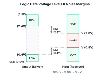
      The key design decision in digital electronics is to represent continuous physical quantities (voltages) with discrete logical values. A voltage above a certain threshold is interpreted as logic 1; below a different threshold, logic 0. The region between these thresholds is forbidden during normal operation and is only passed through transiently during switching. This discretisation is what gives digital circuits their noise immunity and makes reliable system design possible.

      Course Aims

      This course aims to familiarise students with:

      • Combinational logic circuits: circuits whose output depends solely on the current inputs (no memory)
      • Sequential logic circuits: circuits whose output depends on current inputs and past history (they contain memory)
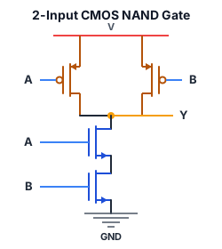
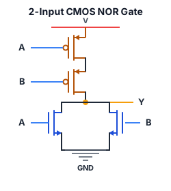
      • How digital logic gates are built using transistors (CMOS)
      • Simple processor architectures
      • The design, build, and testing of digital logic systems

      Course Structure (12 Lectures)

      1. Combinational logic foundations: logic gates, Boolean algebra, De Morgan’s theorem, consensus theorem
      2. Logic minimisation: truth tables, normal forms, Karnaugh maps, don’t-care conditions, Quine-McCluskey
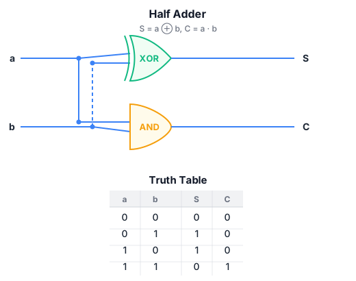
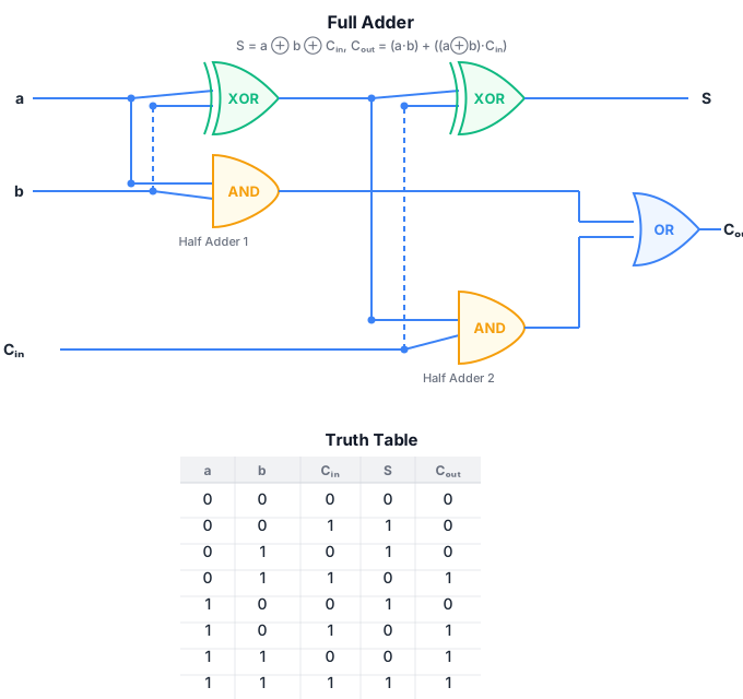
      3. Binary adders: half and full adders, ripple carry, fast carry generation
      4. Multilevel logic and hazards: beyond two-level logic, propagation delay, static and dynamic hazards, hazard removal
      5. Beyond simple logic gates: multiplexers, decoders, ROMs, PLAs, PALs, tristate buffers
      6. Sequential logic: latches, flip-flops, counters, shift registers
      7. FSM design: synchronous finite state machines, state diagrams, excitation tables
      8. Logic implementation technologies: CMOS transistors, gate-level implementation
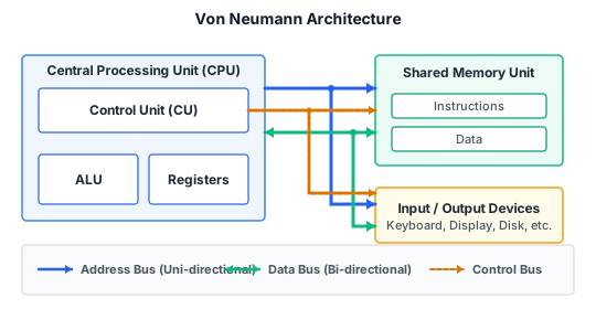
      9. Processor architecture: brief introduction to microprocessor design

      Hardware labs (four workshops of 2.5-3 hours each) run throughout Michaelmas and Lent terms.

      Relationship to Later Courses

      This course is a prerequisite for:

      • Computer Architecture (Part IB): understanding how logic elements combine to form data paths and control units
      • ECAD and Architecture Practical Classes (Part IB): practical design and implementation
      • Advanced Computer Architecture (Part II)
      • Advanced Topics in Computer Architecture (MPhil/Part III)

      The Boolean algebra and logic minimisation techniques taught here are a core competence in Computer Science: they appear in everything from compiler optimisations to database query planning, not just in hardware design.

    • Logic Gates and Truth Tables

      Logic Variables

      Logic variables (also called binary variables or Boolean variables) can only take on two values. Different naming conventions are used interchangeably:

      ConventionValues
      BooleanTRUE, FALSE
      Binary1, 0
      VoltageHIGH, LOW
      SwitchON, OFF

      In electronic circuits these two values are represented by distinct voltage levels, e.g., a high voltage for logic 1 and a low voltage for logic 0. Using only two voltage levels gives digital circuits greater immunity to electrical noise compared with analogue circuits.

      Logic Gates

      A logic gate is a basic electronic circuit with one or more inputs and exactly one output. Gates are the atomic building blocks of all digital logic circuits. There are several ways to represent a logic function: a symbol (circuit diagram), a truth table (exhaustive input-output mapping), and a Boolean expression (algebraic form).

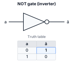
      The NOT Gate (Inverter)

      The NOT gate has one input and one output. Its output is the complement (inverse) of its input.

      NOT gate symbol

      Truth table:

      ay
      01
      10

      Boolean expression: y=aˉy = \bar{a}

      The circle (or “bubble”) on the output of the gate symbol indicates that the output is the complemented (inverted) version of the input. A NOT gate is also called an inverter.

      The AND Gate

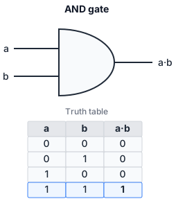
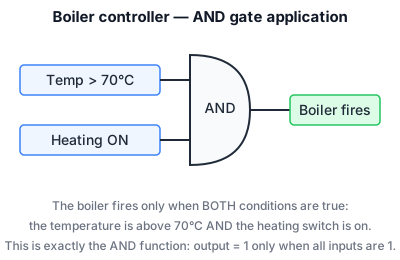
      The AND gate output is TRUE only when all inputs are TRUE.

      AND gate symbol

      Truth table (2-input):

      aby
      000
      010
      100
      111

      Boolean expression: y=aby = a \cdot b (also written as y=aby = ab, or y=aby = a \land b)

      The dot represents the AND operation. For multiple inputs, the AND operation extends naturally: y=abcy = a \cdot b \cdot c \cdot \ldots; the output is 1 only when every input is 1. A 3-input AND gate has 8 rows in its truth table, with only the row (1,1,1) yielding output 1.

      The OR Gate

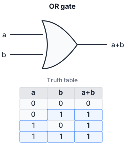
      The OR gate output is TRUE when at least one input is TRUE (the inclusive OR).

      OR gate symbol

      Truth table (2-input):

      aby
      000
      011
      101
      111

      Boolean expression: y=a+by = a + b (also written y=aby = a \lor b)

      The plus sign represents the OR operation (not arithmetic addition). For multiple inputs: y=a+b+c+y = a + b + c + \ldots; the output is 1 if any input is 1.

      The XOR Gate (Exclusive OR)

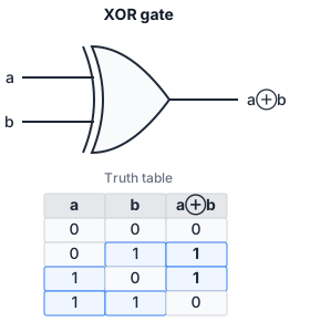
      The XOR gate output is TRUE when an odd number of inputs are TRUE. For two inputs, it is TRUE when exactly one input is TRUE (but not both).

      XOR gate symbol

      Truth table (2-input):

      aby
      000
      011
      101
      110

      Boolean expression: y=ab=abˉ+aˉby = a \oplus b = a \cdot \bar{b} + \bar{a} \cdot b

      The XOR can be thought of as “a OR b but NOT both”, i.e., detecting inequality: y=1y = 1 iff aba \neq b.

      The NAND Gate (NOT AND)

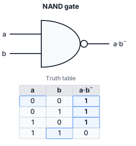
      The NAND gate is an AND gate followed by a NOT. Its output is FALSE only when all inputs are TRUE.

      NAND gate symbol

      Truth table (2-input):

      aby
      001
      011
      101
      110

      Boolean expression: y=aby = \overline{a \cdot b}

      Equivalently, y=aˉ+bˉy = \bar{a} + \bar{b} (by De Morgan’s theorem, see De Morgan’s Theorem). So y is TRUE if a is FALSE or b is FALSE (or both).

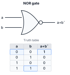
      The NOR Gate (NOT OR)

      The NOR gate is an OR gate followed by a NOT. Its output is TRUE only when all inputs are FALSE.

      NOR gate symbol

      Truth table (2-input):

      aby
      001
      010
      100
      110

      Boolean expression: y=a+by = \overline{a + b}

      Equivalently, y=aˉbˉy = \bar{a} \cdot \bar{b} (by De Morgan’s theorem). So y is TRUE only if a is FALSE AND b is FALSE.

      Universal Gates: NAND and NOR

      Any Boolean function can be built using only NAND gates, or using only NOR gates. NAND and NOR are therefore called universal gates. This is important in practice because NAND and NOR gates are simpler to fabricate in many transistor technologies (particularly CMOS). The proof is straightforward: we can construct NOT, AND, and OR from NAND alone, and since {NOT, AND, OR} is functionally complete, NAND must be too.

      Building NOT from NAND: tie both inputs together: aa=aˉ\overline{a \cdot a} = \bar{a}.

      Building AND from NAND: a NAND followed by a NOT (which is itself a NAND): ab=ab\overline{\overline{a \cdot b}} = a \cdot b.

      Building OR from NAND: apply De Morgan: a+b=aˉbˉa + b = \overline{\bar{a} \cdot \bar{b}}, which is a NAND of two complemented inputs (each complement is itself a NAND).

      Similar constructions work for NOR.

      Worked Example: Boiler Controller

      Consider a heating boiler with the following inputs:

      • bb: chimney is blocked (1 = blocked)
      • cc: house is cold (1 = cold)
      • pp: pilot light is lit (1 = lit)
      • hh: overheat sensor triggered (1 = overheated)

      Output vv: open the main fuel valve to start the boiler (1 = open).

      The valve should open if and only if: the chimney is NOT blocked AND the house is cold AND the pilot light is lit, BUT NOT if the overheat sensor is triggered.

      Boolean expression:

      v=bˉcphˉv = \bar{b} \cdot c \cdot p \cdot \bar{h}

      Boiler controller gate implementation

      The circuit uses one NOT gate (for bˉ\bar{b}), one NOT gate (for hˉ\bar{h}), and one 4-input AND gate. If only 2-input AND gates are available, the three AND terms are cascaded: ((bˉc)p)hˉ((\bar{b} \cdot c) \cdot p) \cdot \bar{h}.

      Combining Gates: Building z=(a)(a+b)z = (\overline{a}) \cdot (a + b)

      We will show how a more complex Boolean expression is implemented by connecting simpler gates. The expression z=aˉ(a+b)z = \bar{a} \cdot (a + b) involves NOT, AND, and OR operations. The circuit diagram consists of: input aa splits into two paths; one path goes through a NOT gate producing aˉ\bar{a}; the other path goes together with bb into an OR gate producing (a+b)(a + b); the outputs of the NOT and OR gates are fed into an AND gate producing the final output zz.

      Truth Table Construction

      To build the truth table for this expression, evaluate it for every combination of the inputs aa and bb:

      1. List all input combinations: for nn inputs there are 2n2^n rows. Here n=2n = 2, so 4 rows.
      2. For each row, compute intermediate sub-expressions.
      3. Combine sub-expressions to get the final output.
      abaˉ\bar{a}a+ba + bz=aˉ(a+b)z = \bar{a} \cdot (a + b)
      001010=01 \cdot 0 = 0
      011111=11 \cdot 1 = 1
      100101=00 \cdot 1 = 0
      110101=00 \cdot 1 = 0

      So zz is 1 only when a=0a = 0 and b=1b = 1. This is exactly z=aˉbz = \bar{a} \cdot b, which can be verified algebraically:

      z=aˉ(a+b)=aˉa+aˉb=0+aˉb=aˉbz = \bar{a} \cdot (a + b) = \bar{a} \cdot a + \bar{a} \cdot b = 0 + \bar{a} \cdot b = \bar{a} \cdot b

      This simplification shows that the OR gate (and the second path from aa) was redundant. The truth table reveals this directly: the only row where z=1z = 1 corresponds to aˉb\bar{a} \cdot b. This is a preview of Boolean algebra simplification, treated fully in the next note.

      Gate-Level Equivalences via De Morgan

      De Morgan’s theorem gives us important equivalences between gate types:

      • An AND gate with bubbles on both inputs is equivalent to a NOR gate: aˉbˉ=a+b\overline{\bar{a} \cdot \bar{b}} = a + b.
      • An OR gate with bubbles on both inputs is equivalent to a NAND gate: aˉ+bˉ=ab\overline{\bar{a} + \bar{b}} = a \cdot b.
      • An AND gate with a bubble on its output is a NAND gate.
      • An OR gate with a bubble on its output is a NOR gate.

      Two consecutive bubbles (complement operations) cancel: a bubble on an input followed by a bubble on the output of the same gate has no net logical effect. This “bubble pushing” technique is a practical method for converting between gate types and is explored in depth in the De Morgan’s Theorem note.

    • Boolean Algebra

      Overview

      Boolean algebra is the mathematical framework for reasoning about logic functions. It operates on binary variables with the operations AND (·), OR (+), and NOT (overbar). The precedence rule is: NOT binds tightest, then AND, then OR. So ab+ca \cdot b + c means (ab)+c(a \cdot b) + c, not a(b+c)a \cdot (b + c).

      A combinational logic circuit has no internal stored state (no memory); its output depends solely on its current inputs. Boolean algebra describes the behaviour of such circuits and allows us to simplify them.

      Basic Identities

      Identities Involving Constants

      NameIdentityMeaning
      OR with 0a+0=aa + 0 = aOR-ing with FALSE leaves aa unchanged
      AND with 0a0=0a \cdot 0 = 0AND-ing with FALSE always gives FALSE
      OR with 1a+1=1a + 1 = 1OR-ing with TRUE always gives TRUE
      AND with 1a1=aa \cdot 1 = aAND-ing with TRUE leaves aa unchanged

      Complementation

      NameIdentityMeaning
      Complementa+aˉ=1a + \bar{a} = 1A variable OR its complement is always TRUE
      aaˉ=0a \cdot \bar{a} = 0A variable AND its complement is always FALSE

      Idempotence

      NameIdentityMeaning
      a+a=aa + a = aOR-ing a variable with itself gives the variable
      aa=aa \cdot a = aAND-ing a variable with itself gives the variable

      Involution (Double Complement)

      a=a\overline{\overline{a}} = a

      Complementing twice returns the original value. This is also why two bubbles in series cancel.

      Commutative, Associative, and Distributive Laws

      Commutative

      a+b=b+aa + b = b + a ab=baa \cdot b = b \cdot a

      The order of operands does not matter for AND or OR.

      Associative

      (a+b)+c=a+(b+c)(a + b) + c = a + (b + c) (ab)c=a(bc)(a \cdot b) \cdot c = a \cdot (b \cdot c)

      Grouping does not matter, so we write a+b+ca + b + c or abca \cdot b \cdot c without parentheses.

      Distributive

      Boolean algebra has two distributive laws, and the second one has no analogue in ordinary algebra:

      a(b+c)=(ab)+(ac)a \cdot (b + c) = (a \cdot b) + (a \cdot c) a+(bc)=(a+b)(a+c)(NEW: not true in ordinary algebra)a + (b \cdot c) = (a + b) \cdot (a + c) \qquad \text{(NEW: not true in ordinary algebra)}

      The second law can be verified by truth table or algebraic expansion:

      (a+b)(a+c)=aa+ac+ba+bc=a+ac+ab+bc=a+bc(a + b) \cdot (a + c) = a \cdot a + a \cdot c + b \cdot a + b \cdot c = a + a \cdot c + a \cdot b + b \cdot c = a + b \cdot c

      where the last step uses absorption (below).

      Absorption Laws

      a+(ac)=aa + (a \cdot c) = a a(a+c)=aa \cdot (a + c) = a

      Proof of the first: a+ac=a1+ac=a(1+c)=a1=aa + a \cdot c = a \cdot 1 + a \cdot c = a \cdot (1 + c) = a \cdot 1 = a.

      Proof of the second: a(a+c)=aa+ac=a+ac=aa \cdot (a + c) = a \cdot a + a \cdot c = a + a \cdot c = a (using idempotence and the first absorption law).

      Intuition: in a+aca + a \cdot c, if a=1a = 1 the output is 1 regardless of cc; if a=0a = 0 then ac=0a \cdot c = 0 and 0+0=00 + 0 = 0. So the output is always exactly aa.

      De Morgan’s Theorem (Preview)

      De Morgan’s theorem tells us how to push complements through AND and OR:

      a+b=aˉbˉ\overline{a + b} = \bar{a} \cdot \bar{b} ab=aˉ+bˉ\overline{a \cdot b} = \bar{a} + \bar{b}

      This is treated in full in the De Morgan’s Theorem note. For now, note its algebraic role: it allows us to transform AND expressions into OR expressions and vice versa.

      Worked Simplification Examples

      Example 1: abc+abcˉa \cdot b \cdot c + a \cdot b \cdot \bar{c}

      abc+abcˉ=ab(c+cˉ)(factor ab)=ab1(complement: c+cˉ=1)=ab\begin{aligned} a \cdot b \cdot c + a \cdot b \cdot \bar{c} &= a \cdot b \cdot (c + \bar{c}) \quad \text{(factor } a \cdot b \text{)} \\ &= a \cdot b \cdot 1 \quad \text{(complement: } c + \bar{c} = 1 \text{)} \\ &= a \cdot b \end{aligned}

      The two terms differ only in the complementation of cc; they combine to eliminate cc entirely. This technique, factoring out common literals and applying x+xˉ=1x + \bar{x} = 1, is the core algebraic simplification method.

      Example 2: Show a(aˉ+b)=aba \cdot (\bar{a} + b) = a \cdot b

      a(aˉ+b)=aaˉ+ab(distribute a)=0+ab(complement: aaˉ=0)=ab\begin{aligned} a \cdot (\bar{a} + b) &= a \cdot \bar{a} + a \cdot b \quad \text{(distribute } a \text{)} \\ &= 0 + a \cdot b \quad \text{(complement: } a \cdot \bar{a} = 0 \text{)} \\ &= a \cdot b \end{aligned}

      The term aaˉa \cdot \bar{a} vanishes because a variable AND its complement is always 0.

      Example 3: Show a+(aˉb)=a+ba + (\bar{a} \cdot b) = a + b

      a+(aˉb)=(a+aˉ)(a+b)(distribute OR over AND)=1(a+b)(complement: a+aˉ=1)=a+b\begin{aligned} a + (\bar{a} \cdot b) &= (a + \bar{a}) \cdot (a + b) \quad \text{(distribute OR over AND)} \\ &= 1 \cdot (a + b) \quad \text{(complement: } a + \bar{a} = 1 \text{)} \\ &= a + b \end{aligned}

      This uses the “new” distributive law a+(bc)=(a+b)(a+c)a + (b \cdot c) = (a + b) \cdot (a + c), which has no parallel in ordinary arithmetic.

      Example 4: Simplify xy+yz+xz+xyzx \cdot y + y \cdot z + x \cdot z + x \cdot y \cdot z

      We use the technique of expanding each term to include all variables (by multiplying terms by (v+vˉ)=1(v + \bar{v}) = 1 for missing variables), then cancelling:

      First, expand every term to include xx, yy, and zz:

      • xy=xy(z+zˉ)=xyz+xyzˉx \cdot y = x \cdot y \cdot (z + \bar{z}) = x \cdot y \cdot z + x \cdot y \cdot \bar{z}
      • yz=(x+xˉ)yz=xyz+xˉyzy \cdot z = (x + \bar{x}) \cdot y \cdot z = x \cdot y \cdot z + \bar{x} \cdot y \cdot z
      • xz=x(y+yˉ)z=xyz+xyˉzx \cdot z = x \cdot (y + \bar{y}) \cdot z = x \cdot y \cdot z + x \cdot \bar{y} \cdot z
      • xyzx \cdot y \cdot z is already fully expanded

      Now list all minterms:

      xyzx \cdot y \cdot z (from xyxy), xyzˉx \cdot y \cdot \bar{z} (from xyxy), xyzx \cdot y \cdot z (from yzyz), xˉyz\bar{x} \cdot y \cdot z (from yzyz), xyzx \cdot y \cdot z (from xzxz), xyˉzx \cdot \bar{y} \cdot z (from xzxz), xyzx \cdot y \cdot z (from xyzxyz).

      Removing duplicates, the distinct minterms are: xyzx \cdot y \cdot z, xyzˉx \cdot y \cdot \bar{z}, xˉyz\bar{x} \cdot y \cdot z, xyˉzx \cdot \bar{y} \cdot z.

      Group:

      xyz+xyzˉ+xˉyz+xyˉzx \cdot y \cdot z + x \cdot y \cdot \bar{z} + \bar{x} \cdot y \cdot z + x \cdot \bar{y} \cdot z =xy(z+zˉ)+yz(x+xˉ)= x \cdot y \cdot (z + \bar{z}) + y \cdot z \cdot (x + \bar{x}) =xy+yz= x \cdot y + y \cdot z

      So the original expression simplifies to xy+yzx \cdot y + y \cdot z.

      Consensus Theorem

      The consensus theorem states:

      ab+aˉc+bc=ab+aˉca \cdot b + \bar{a} \cdot c + b \cdot c = a \cdot b + \bar{a} \cdot c

      The term bcb \cdot c is the consensus of aba \cdot b and aˉc\bar{a} \cdot c: it is formed by taking the AND of all literals that appear in both terms, excluding the variable and its complement (aa and aˉ\bar{a}). The consensus term is redundant and can be added or removed without changing the function.

      Proof

      ab+aˉc+bc=ab+aˉc+bc(a+aˉ)(multiply bc by 1)=ab+aˉc+abc+aˉbc(distribute)=(ab+abc)+(aˉc+aˉbc)(rearrange)=ab(1+c)+aˉc(1+b)(factor)=ab+aˉc(since 1+x=1)\begin{aligned} a \cdot b + \bar{a} \cdot c + b \cdot c &= a \cdot b + \bar{a} \cdot c + b \cdot c \cdot (a + \bar{a}) \quad \text{(multiply } b \cdot c \text{ by 1)} \\ &= a \cdot b + \bar{a} \cdot c + a \cdot b \cdot c + \bar{a} \cdot b \cdot c \quad \text{(distribute)} \\ &= (a \cdot b + a \cdot b \cdot c) + (\bar{a} \cdot c + \bar{a} \cdot b \cdot c) \quad \text{(rearrange)} \\ &= a \cdot b \cdot (1 + c) + \bar{a} \cdot c \cdot (1 + b) \quad \text{(factor)} \\ &= a \cdot b + \bar{a} \cdot c \quad \text{(since } 1 + x = 1 \text{)} \end{aligned}

      Dual Form

      The dual of the consensus theorem (swap AND with OR, 0 with 1) gives:

      (a+b)(aˉ+c)(b+c)=(a+b)(aˉ+c)(a + b) \cdot (\bar{a} + c) \cdot (b + c) = (a + b) \cdot (\bar{a} + c)

      The dual can be proven by applying De Morgan’s theorem to both sides of the original, or by a similar algebraic expansion.

      Using Consensus: Adding and Eliminating Terms

      The theorem works in both directions:

      • Elimination: If you see ab+aˉc+bca \cdot b + \bar{a} \cdot c + b \cdot c, remove bcb \cdot c to get ab+aˉca \cdot b + \bar{a} \cdot c.
      • Addition: If you have ab+aˉca \cdot b + \bar{a} \cdot c and need to combine it with other terms, you can add bcb \cdot c without changing the function (useful for hazard removal, see Hazard Removal).

      Example: Simplify ab+aˉc+bc+bˉc+abˉa \cdot b + \bar{a} \cdot c + b \cdot c + \bar{b} \cdot c + a \cdot \bar{b}.

      First, identify consensus terms. The term bcb \cdot c is the consensus of aba \cdot b and aˉc\bar{a} \cdot c, so it can be removed. After removal: ab+aˉc+bˉc+abˉa \cdot b + \bar{a} \cdot c + \bar{b} \cdot c + a \cdot \bar{b}.

      Now examine what remains. The term bˉc\bar{b} \cdot c and abˉa \cdot \bar{b} look for consensus with others. But note that aˉc+bˉc=aˉc\bar{a} \cdot c + \bar{b} \cdot c = \bar{a} \cdot c does not directly give consensus removal. In this case further algebraic inspection (or a K-map) reveals the minimal form.

      Example with clear elimination: Simplify ab+aˉc+bc+bˉca \cdot b + \bar{a} \cdot c + b \cdot c + \bar{b} \cdot c.

      The term bcb \cdot c is consensus of aba \cdot b and aˉc\bar{a} \cdot c (remove it). Check if bˉc\bar{b} \cdot c is consensus of any pair: no obvious pair. Result: ab+aˉc+bˉca \cdot b + \bar{a} \cdot c + \bar{b} \cdot c. Further, note aˉc+bˉc=(aˉ+bˉ)c\bar{a} \cdot c + \bar{b} \cdot c = (\bar{a} + \bar{b}) \cdot c, which cannot be simplified further without additional context. The final expression depends on the specific terms.

      Summary of Boolean Laws

      LawOR formAND form
      Identitya+0=aa + 0 = aa1=aa \cdot 1 = a
      Nulla+1=1a + 1 = 1a0=0a \cdot 0 = 0
      Idempotencea+a=aa + a = aaa=aa \cdot a = a
      Complementa+aˉ=1a + \bar{a} = 1aaˉ=0a \cdot \bar{a} = 0
      Involutiona=a\overline{\overline{a}} = a
      Commutativea+b=b+aa + b = b + aab=baa \cdot b = b \cdot a
      Associative(a+b)+c=a+(b+c)(a+b)+c = a+(b+c)(ab)c=a(bc)(a \cdot b) \cdot c = a \cdot (b \cdot c)
      Distributivea+bc=(a+b)(a+c)a + b \cdot c = (a+b) \cdot (a+c)a(b+c)=ab+aca \cdot (b+c) = a \cdot b + a \cdot c
      Absorptiona+ab=aa + a \cdot b = aa(a+b)=aa \cdot (a+b) = a
      De Morgana+b=aˉbˉ\overline{a+b} = \bar{a} \cdot \bar{b}ab=aˉ+bˉ\overline{a \cdot b} = \bar{a} + \bar{b}
      Consensusab+aˉc+bc=ab+aˉca \cdot b + \bar{a} \cdot c + b \cdot c = a \cdot b + \bar{a} \cdot c(a+b)(aˉ+c)(b+c)=(a+b)(aˉ+c)(a+b) \cdot (\bar{a}+c) \cdot (b+c) = (a+b) \cdot (\bar{a}+c)
    • De Morgan's Theorem

      Statement of the Theorem

      De Morgan’s theorem describes how to distribute a complement (NOT) over an AND or OR operation:

      ab=aˉ+bˉ\overline{a \cdot b} = \bar{a} + \bar{b}

      a+b=aˉbˉ\overline{a + b} = \bar{a} \cdot \bar{b}

      In words:

      • The complement of a product equals the sum of the complements: ab=aˉ+bˉ\overline{a \cdot b} = \bar{a} + \bar{b}.
      • The complement of a sum equals the product of the complements: a+b=aˉbˉ\overline{a + b} = \bar{a} \cdot \bar{b}.

      For the general form with nn variables:

      abc=aˉ+bˉ+cˉ+\overline{a \cdot b \cdot c \cdot \ldots} = \bar{a} + \bar{b} + \bar{c} + \ldots

      a+b+c+=aˉbˉcˉ\overline{a + b + c + \ldots} = \bar{a} \cdot \bar{b} \cdot \bar{c} \cdot \ldots

      Truth Table Verification

      For two variables, both forms can be verified exhaustively:

      abab\overline{a \cdot b}aˉ+bˉ\bar{a} + \bar{b}a+b\overline{a + b}aˉbˉ\bar{a} \cdot \bar{b}
      001111
      011100
      101100
      110000

      The columns for ab\overline{a \cdot b} and aˉ+bˉ\bar{a} + \bar{b} are identical, confirming the first form. The columns for a+b\overline{a + b} and aˉbˉ\bar{a} \cdot \bar{b} are identical, confirming the second form.

      Inductive Extension to More Variables

      The theorem extends to any number of variables by induction. For three variables:

      a+b+c=(a+b)+c=a+bcˉ=(aˉbˉ)cˉ=aˉbˉcˉ\overline{a + b + c} = \overline{(a + b) + c} = \overline{a + b} \cdot \bar{c} = (\bar{a} \cdot \bar{b}) \cdot \bar{c} = \bar{a} \cdot \bar{b} \cdot \bar{c}

      The key step applies the two-variable form treating (a+b)(a + b) as a single variable combined with cc.

      Similarly for the AND form:

      abc=(ab)c=ab+cˉ=(aˉ+bˉ)+cˉ=aˉ+bˉ+cˉ\overline{a \cdot b \cdot c} = \overline{(a \cdot b) \cdot c} = \overline{a \cdot b} + \bar{c} = (\bar{a} + \bar{b}) + \bar{c} = \bar{a} + \bar{b} + \bar{c}

      Practical Rule for Application

      To apply De Morgan’s theorem to a Boolean expression:

      1. Change all ANDs to ORs (and vice versa).
      2. Complement each individual variable (put a bar over every literal).
      3. Complement the entire expression (put a bar over the whole thing).

      Example: Apply De Morgan to a+bca + b \cdot c.

      Step 1: change OR to AND, AND to OR: a(b+c)a \cdot (b + c) Step 2: complement each variable: aˉ(bˉ+cˉ)\bar{a} \cdot (\bar{b} + \bar{c}) Step 3: complement the whole: aˉ(bˉ+cˉ)\overline{\bar{a} \cdot (\bar{b} + \bar{c})}

      So a+bc=aˉ(bˉ+cˉ)\overline{a + b \cdot c} = \overline{\bar{a} \cdot (\bar{b} + \bar{c})}. We can then simplify the right-hand side further by applying De Morgan again:

      aˉ(bˉ+cˉ)=aˉ+bˉ+cˉ=a+(bc)\overline{\bar{a} \cdot (\bar{b} + \bar{c})} = \overline{\bar{a}} + \overline{\bar{b} + \bar{c}} = a + (b \cdot c)

      Which returns us to the original, confirming correctness.

      More usefully, De Morgan can simplify: a+bc=aˉbc=aˉ(bˉ+cˉ)\overline{a + b \cdot c} = \bar{a} \cdot \overline{b \cdot c} = \bar{a} \cdot (\bar{b} + \bar{c}).

      Worked Algebraic Example

      Simplify ab+a(b+c)+b(b+c)\overline{a \cdot b + a \cdot (b + c) + b \cdot (b + c)}.

      Step 1: Apply De Morgan to the whole expression (impossible directly because it’s a sum of three terms). Instead, simplify inside first.

      Inside: ab+a(b+c)+b(b+c)a \cdot b + a \cdot (b + c) + b \cdot (b + c)

      Simplify each term algebraically before applying De Morgan:

      ab+ab+c+bb+ca \cdot b + a \cdot \overline{b + c} + b \cdot \overline{b + c}

      Apply De Morgan: b+c=bˉcˉ\overline{b + c} = \bar{b} \cdot \bar{c}.

      =ab+abˉcˉ+bbˉcˉ= a \cdot b + a \cdot \bar{b} \cdot \bar{c} + b \cdot \bar{b} \cdot \bar{c}

      Note bbˉ=0b \cdot \bar{b} = 0, so the third term vanishes:

      =ab+abˉcˉ= a \cdot b + a \cdot \bar{b} \cdot \bar{c}

      Factor aa: =a(b+bˉcˉ)= a \cdot (b + \bar{b} \cdot \bar{c})

      Using the distributive law x+xˉy=x+yx + \bar{x} \cdot y = x + y (proved in the Boolean Algebra note):

      =a(b+cˉ)= a \cdot (b + \bar{c})

      Bubble Logic: Gate Equivalences

      De Morgan’s theorem has an elegant interpretation in terms of gate symbols. The “bubble” on a gate input or output represents complementation.

      Rule 1: Two Bubbles Cancel

      Two bubbles in series (an input bubble feeding into an output bubble along the same wire) cancel and have no logical effect:

      x=x\overline{\overline{x}} = x

      Rule 2: AND with Inverted Inputs = NOR

      An AND gate with bubbles on all inputs:

      aˉbˉ=aˉˉ+bˉˉ=a+b\overline{\bar{a} \cdot \bar{b}} = \bar{\bar{a}} + \bar{\bar{b}} = a + b

      So an AND gate with inverted inputs is functionally a NOR gate (and equivalently, a NOR gate with inverted inputs is an AND gate).

      Rule 3: OR with Inverted Inputs = NAND

      An OR gate with bubbles on all inputs:

      aˉ+bˉ=aˉˉbˉˉ=ab\overline{\bar{a} + \bar{b}} = \bar{\bar{a}} \cdot \bar{\bar{b}} = a \cdot b

      So an OR gate with inverted inputs is functionally a NAND gate.

      Rule 4: Bubble Through a Gate

      Moving a bubble from output to inputs changes the gate type:

      • NAND: AND gate followed by bubble → bubble input OR gate: ab=aˉ+bˉ\overline{a \cdot b} = \bar{a} + \bar{b}
      • NOR: OR gate followed by bubble → bubble input AND gate: a+b=aˉbˉ\overline{a + b} = \bar{a} \cdot \bar{b}

      Example 1: Implementing f=ab+cdf = a \cdot b + c \cdot d Using Only NAND Gates

      The expression f=ab+cdf = a \cdot b + c \cdot d is in SOP form: two AND terms OR-ed together.

      Direct implementation uses two AND gates and one OR gate.

      NAND-only implementation: Apply De Morgan by double-complementing:

      f=ab+cdf = a \cdot b + c \cdot d f=ab+cdf = \overline{\overline{a \cdot b + c \cdot d}} f=abcdf = \overline{\overline{a \cdot b} \cdot \overline{c \cdot d}}

      The outer complement tells us to use a NAND gate. Its inputs are ab\overline{a \cdot b} and cd\overline{c \cdot d}, each of which is the output of a NAND gate. So the circuit is: three NAND gates. Two NAND gates feed into a third NAND gate.

      Gate 1: NAND of aa and bb produces ab\overline{a \cdot b}. Gate 2: NAND of cc and dd produces cd\overline{c \cdot d}. Gate 3: NAND of the two intermediate signals produces abcd=ab+cd\overline{\overline{a \cdot b} \cdot \overline{c \cdot d}} = a \cdot b + c \cdot d.

      Example 2: Implementing f=(a+b)(c+d)f = (a + b) \cdot (c + d) Using Only NOR Gates

      The expression f=(a+b)(c+d)f = (a + b) \cdot (c + d) is in POS form: two OR terms AND-ed together.

      NOR-only implementation: Double-complement and apply De Morgan:

      f=(a+b)(c+d)f = (a + b) \cdot (c + d) f=(a+b)(c+d)f = \overline{\overline{(a + b) \cdot (c + d)}} f=a+b+c+df = \overline{\overline{a + b} + \overline{c + d}}

      Now the outer complement is a NOR gate. Its inputs are a+b\overline{a + b} and c+d\overline{c + d}, each produced by a NOR gate. So three NOR gates in total.

      Gate 1: NOR of aa and bb produces a+b\overline{a + b}. Gate 2: NOR of cc and dd produces c+d\overline{c + d}. Gate 3: NOR of the two intermediate signals produces a+b+c+d=(a+b)(c+d)\overline{\overline{a + b} + \overline{c + d}} = (a + b) \cdot (c + d).

      Summary of Gate Transformations

      Original gateWith bubbles on inputsEquivalent gate
      ANDBubbles on both inputsNOR
      ORBubbles on both inputsNAND
      NANDBubbles on both inputsOR
      NORBubbles on both inputsAND

      These transformations are the foundation of bubble pushing: a technique for converting a circuit from one gate type to another while preserving the logic function. They are essential when a designer must implement a circuit using only one type of gate (e.g., NAND-only or NOR-only designs, which are common in CMOS).

    • Consensus Theorem

      Statement

      The consensus theorem in its most common form states:

      ab+aˉc+bc=ab+aˉca \cdot b + \bar{a} \cdot c + b \cdot c = a \cdot b + \bar{a} \cdot c

      The term bcb \cdot c is called the consensus term. It is formed by taking the AND of the terms that remain after removing the variable and its complement from the two product terms aba \cdot b and aˉc\bar{a} \cdot c: strip aa from aba \cdot b to get bb, strip aˉ\bar{a} from aˉc\bar{a} \cdot c to get cc, and AND them to get bcb \cdot c.

      The dual form (swap AND with OR):

      (a+b)(aˉ+c)(b+c)=(a+b)(aˉ+c)(a + b) \cdot (\bar{a} + c) \cdot (b + c) = (a + b) \cdot (\bar{a} + c)

      Proof via Boolean Algebra

      Starting from the left-hand side:

      ab+aˉc+bc=ab+aˉc+bc(a+aˉ)=ab+aˉc+abc+aˉbc=(ab+abc)+(aˉc+aˉbc)=ab(1+c)+aˉc(1+b)=ab1+aˉc1=ab+aˉc\begin{aligned} a \cdot b + \bar{a} \cdot c + b \cdot c &= a \cdot b + \bar{a} \cdot c + b \cdot c \cdot (a + \bar{a}) \\ &= a \cdot b + \bar{a} \cdot c + a \cdot b \cdot c + \bar{a} \cdot b \cdot c \\ &= (a \cdot b + a \cdot b \cdot c) + (\bar{a} \cdot c + \bar{a} \cdot b \cdot c) \\ &= a \cdot b \cdot (1 + c) + \bar{a} \cdot c \cdot (1 + b) \\ &= a \cdot b \cdot 1 + \bar{a} \cdot c \cdot 1 \\ &= a \cdot b + \bar{a} \cdot c \end{aligned}

      The critical trick is multiplying bcb \cdot c by (a+aˉ)=1(a + \bar{a}) = 1. This expands the consensus term into two terms, each of which is absorbed by one of the original product terms.

      Proof via Truth Table

      Build the truth table for all three input variables and compute both sides:

      abcaba \cdot baˉc\bar{a} \cdot cbcb \cdot cLHS (ab+aˉc+bcab + \bar{a}c + bc)RHS (ab+aˉcab + \bar{a}c)
      00000000
      00101011
      01000000
      01101111
      10000000
      10100000
      11010011
      11110111

      The columns for LHS and RHS are identical, confirming the theorem. Notice that bcb \cdot c is 1 only in rows where either aba \cdot b or aˉc\bar{a} \cdot c is already 1, so it never adds a new 1 to the function.

      Proof via Karnaugh Map Preview

      Plot the function f=ab+aˉc+bcf = a \cdot b + \bar{a} \cdot c + b \cdot c on a K-map (3 variables: a, b, c). The K-map for a 3-variable function uses Gray code ordering:

      abc000111100011010011\begin{array}{c|cccc} a \setminus bc & 00 & 01 & 11 & 10 \\ \hline 0 & 0 & 1 & 1 & 0 \\ 1 & 0 & 0 & 1 & 1 \end{array}

      The term aba \cdot b (1 when a=1, b=1, any c) covers cells (a=1, b=1, c=0) and (a=1, b=1, c=1), i.e., bc=10 and bc=11 in the second row. Both are 1.

      The term aˉc\bar{a} \cdot c (1 when a=0, c=1, any b) covers cells (a=0, b=0, c=1) and (a=0, b=1, c=1), i.e., bc=01 and bc=11 in the first row. Both are 1.

      The term bcb \cdot c (1 when b=1, c=1, any a) covers (a=0, b=1, c=1) and (a=1, b=1, c=1). But both of these cells are already covered by aˉc\bar{a} \cdot c and aba \cdot b respectively. So bcb \cdot c is redundant: it covers no minterms that are not already covered. This visual verification matches the algebraic proof: the consensus term is always redundant on a K-map because its cells are a subset of the union of the two generating terms’ cells.

      How to Identify a Consensus Term

      Given two product terms, a consensus term exists if they contain exactly one variable that appears complemented in one term and uncomplemented in the other. For aba \cdot b and aˉc\bar{a} \cdot c: the variable aa appears uncomplemented in the first and complemented in the second. The consensus is formed by AND-ing the remaining literals: bcb \cdot c.

      Example: xyˉzx \cdot \bar{y} \cdot z and xˉwz\bar{x} \cdot w \cdot z

      • Conflicting variable: xx (uncomplemented vs complemented)
      • Remaining literals: yˉz\bar{y} \cdot z and wzw \cdot z
      • Consensus term: yˉzw\bar{y} \cdot z \cdot w (AND of all remaining literals from both terms)

      Using Consensus to Simplify

      Elimination of Consensus Terms

      If you find a consensus term in an expression, you can delete it without changing the function:

      ab+aˉc+bc=ab+aˉca \cdot b + \bar{a} \cdot c + b \cdot c = a \cdot b + \bar{a} \cdot c

      Example: Simplify ab+aˉc+bc+bˉc+abˉa \cdot b + \bar{a} \cdot c + b \cdot c + \bar{b} \cdot c + a \cdot \bar{b}.

      In this expression, bcb \cdot c is the consensus of aba \cdot b and aˉc\bar{a} \cdot c, so eliminate it.

      Now examine the remaining expression: ab+aˉc+bˉc+abˉa \cdot b + \bar{a} \cdot c + \bar{b} \cdot c + a \cdot \bar{b}.

      Looking for other consensus terms: abˉa \cdot \bar{b} and aˉc\bar{a} \cdot c do not share a conflicting variable (the variables aa and bb in the first, aˉ\bar{a} and cc in the second; aa conflicts, leaving bˉ\bar{b} and cc; consensus would be bˉc\bar{b} \cdot c, which is already present!). So bˉc\bar{b} \cdot c is the consensus of abˉa \cdot \bar{b} and aˉc\bar{a} \cdot c, and can be removed.

      Final expression: ab+aˉc+abˉa \cdot b + \bar{a} \cdot c + a \cdot \bar{b}.

      Adding Consensus Terms for Simplification

      Sometimes it is useful to add a consensus term to enable further simplification. This is non-obvious because adding a term makes the expression larger; but it may allow factoring or combination that yields a net reduction.

      Example: Simplify ab+ac+aˉbca \cdot b + a \cdot c + \bar{a} \cdot b \cdot c.

      Direct simplification does not give much leverage. Add the consensus of aba \cdot b and aca \cdot c: these share aa in common (no conflict), so no consensus between them. The consensus of aba \cdot b and aˉbc\bar{a} \cdot b \cdot c: conflicting variable aa, remaining literals bb from the first and bcb \cdot c from the second; consensus is bbc=bcb \cdot b \cdot c = b \cdot c. Add bcb \cdot c:

      ab+ac+aˉbc+bca \cdot b + a \cdot c + \bar{a} \cdot b \cdot c + b \cdot c =ab+ac+bc(aˉ+1)= a \cdot b + a \cdot c + b \cdot c \cdot (\bar{a} + 1) =ab+ac+bc= a \cdot b + a \cdot c + b \cdot c =a(b+c)+bc= a \cdot (b + c) + b \cdot c

      (Better example with a real simplification):

      Example: Simplify abˉ+aˉb+acˉa \cdot \bar{b} + \bar{a} \cdot b + a \cdot \bar{c}.

      Check consensus: abˉa \cdot \bar{b} and aˉb\bar{a} \cdot b have aa conflicting, remaining literals bˉ\bar{b} and bb, consensus bˉb=0\bar{b} \cdot b = 0 (trivial). abˉa \cdot \bar{b} and acˉa \cdot \bar{c} have no conflicting variable (both start with aa). aˉb\bar{a} \cdot b and acˉa \cdot \bar{c} have aa conflicting, remaining bb and cˉ\bar{c}, consensus bcˉb \cdot \bar{c}. Add bcˉb \cdot \bar{c}:

      abˉ+aˉb+acˉ+bcˉa \cdot \bar{b} + \bar{a} \cdot b + a \cdot \bar{c} + b \cdot \bar{c}

      Now acˉ+bcˉ=(a+b)cˉa \cdot \bar{c} + b \cdot \bar{c} = (a + b) \cdot \bar{c}. So:

      =abˉ+aˉb+(a+b)cˉ= a \cdot \bar{b} + \bar{a} \cdot b + (a + b) \cdot \bar{c}

      This may or may not be simpler than the original, depending on the implementation cost metric. The point is that adding a consensus term is a legitimate step that opens up new factoring possibilities.

      Proof of the Dual Form

      The dual of the consensus theorem is:

      (a+b)(aˉ+c)(b+c)=(a+b)(aˉ+c)(a + b) \cdot (\bar{a} + c) \cdot (b + c) = (a + b) \cdot (\bar{a} + c)

      Proof: Start from the left-hand side and apply the distributive law for OR over AND to expand, or apply De Morgan to reduce to the original form:

      Let f=(a+b)(aˉ+c)(b+c)f = (a + b) \cdot (\bar{a} + c) \cdot (b + c). Take the complement:

      fˉ=(a+b)(aˉ+c)(b+c)\bar{f} = \overline{(a + b) \cdot (\bar{a} + c) \cdot (b + c)} fˉ=a+b+aˉ+c+b+c\bar{f} = \overline{a + b} + \overline{\bar{a} + c} + \overline{b + c} fˉ=aˉbˉ+acˉ+bˉcˉ\bar{f} = \bar{a} \cdot \bar{b} + a \cdot \bar{c} + \bar{b} \cdot \bar{c}

      Now apply the original consensus theorem to fˉ\bar{f} (the variables are now aˉ\bar{a}, aa, bˉ\bar{b}, cˉ\bar{c}; the conflicting variable is aˉ/a\bar{a}/a, remaining terms bˉ\bar{b} and cˉ\bar{c}, consensus bˉcˉ\bar{b} \cdot \bar{c}):

      fˉ=aˉbˉ+acˉ\bar{f} = \bar{a} \cdot \bar{b} + a \cdot \bar{c}

      Take the complement again:

      f=aˉbˉ+acˉf = \overline{\bar{a} \cdot \bar{b} + a \cdot \bar{c}} f=aˉbˉacˉf = \overline{\bar{a} \cdot \bar{b}} \cdot \overline{a \cdot \bar{c}} f=(a+b)(aˉ+c)f = (a + b) \cdot (\bar{a} + c)

      Which proves the dual form. This approach (complement, apply the original theorem, complement again) is a general technique for proving the dual of any Boolean identity.

      Extended Consensus: Three or More Consensus Terms

      Consider an expression with three product terms that each conflict with the others in a cycle:

      ab+bc+aca \cdot b + b \cdot c + a \cdot c

      Here the consensus of aba \cdot b and bcb \cdot c (conflicting on bb) leaves aca \cdot c, which is already the third term. The consensus of aba \cdot b and aca \cdot c (conflicting on aa) leaves bcb \cdot c, also present. So with all three terms present, any one can be eliminated as the consensus of the other two: ab+ac=ab+ac+bca \cdot b + a \cdot c = a \cdot b + a \cdot c + b \cdot c, but equally bc+ac=bc+ac+abb \cdot c + a \cdot c = b \cdot c + a \cdot c + a \cdot b. The three-term expression reduces to any two of the three.

      In general, when multiple consensus terms exist, eliminating them iteratively reduces the expression to a form that cannot be further simplified by consensus alone. The order of elimination can affect the intermediate expression but the final minimised form is unique for a given function (up to K-map grouping choices).

      Connection to Hazard Removal

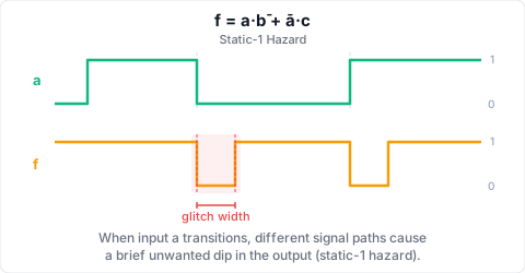
      The consensus theorem is not just a simplification tool. In the context of hazards (see Static and Dynamic Hazards), the consensus term corresponds to a redundant prime implicant that, when added to a circuit, eliminates static hazards. For the function f=abˉ+aˉcf = a \cdot \bar{b} + \bar{a} \cdot c, when b=c=1b = c = 1, a change in aa causes a momentary glitch. Adding the consensus term bcb \cdot c gives f=abˉ+aˉc+bcf = a \cdot \bar{b} + \bar{a} \cdot c + b \cdot c, which is logically identical but hazard-free. The consensus theorem guarantees that adding bcb \cdot c does not change the Boolean function; it only adds a physical gate that holds the output steady during the transition.

  • Logic Minimisation

    Truth tables, disjunctive and conjunctive normal forms (DNF/CNF), minterms and maxterms, Karnaugh maps with SOP and POS simplification, don't-care conditions, and the Quine-McCluskey tabular method

    • Truth Tables and Normal Forms

      Truth Tables

      A truth table exhaustively lists every possible combination of input values and the corresponding output of a Boolean function. For a function of nn variables, the truth table has 2n2^n rows. The rows are conventionally listed in binary counting order (0 to 2n12^n - 1), though other orderings (e.g., Gray code) are sometimes used for specific purposes.

      Example: The function f(x,y,z)=x+yzf(x, y, z) = x + y \cdot z has the following truth table:

      xyzyzy \cdot zf=x+yzf = x + y \cdot z
      00000
      00100
      01000
      01111
      10001
      10101
      11001
      11111

      Minterms

      A minterm of nn Boolean variables is a product (AND) term that includes every variable exactly once, in either complemented or uncomplemented form. For nn variables there are 2n2^n possible minterms.

      Notation: mim_i denotes the minterm corresponding to row ii of the truth table. For a function of 3 variables (xx, yy, zz), with xx as the most significant bit:

      ixyzMinterm mim_i
      0000xˉyˉzˉ\bar{x} \cdot \bar{y} \cdot \bar{z}
      1001xˉyˉz\bar{x} \cdot \bar{y} \cdot z
      2010xˉyzˉ\bar{x} \cdot y \cdot \bar{z}
      3011xˉyz\bar{x} \cdot y \cdot z
      4100xyˉzˉx \cdot \bar{y} \cdot \bar{z}
      5101xyˉzx \cdot \bar{y} \cdot z
      6110xyzˉx \cdot y \cdot \bar{z}
      7111xyzx \cdot y \cdot z

      A minterm mim_i is TRUE (equals 1) for exactly one input combination: the combination corresponding to row ii. Note that yzy \cdot z is NOT a minterm for a 3-variable function because it omits xx; it is simply a product term.

      Disjunctive Normal Form (DNF)

      The Disjunctive Normal Form (DNF), also called Sum of Products (SOP) form, expresses a Boolean function as the OR (sum, disjunction) of its minterms. Specifically:

      f=mifor all i where f=1f = \sum m_i \quad \text{for all } i \text{ where } f = 1

      Using Σ\Sigma notation for brevity: f=Σ(3,4,5,6,7)f = \Sigma(3, 4, 5, 6, 7) means the OR of minterms m3m_3, m4m_4, m5m_5, m6m_6, m7m_7.

      For the example function f=x+yzf = x + y \cdot z above, the rows where f=1f = 1 are 3, 4, 5, 6, 7. The DNF is:

      f=xˉyz+xyˉzˉ+xyˉz+xyzˉ+xyzf = \bar{x} \cdot y \cdot z + x \cdot \bar{y} \cdot \bar{z} + x \cdot \bar{y} \cdot z + x \cdot y \cdot \bar{z} + x \cdot y \cdot z

      DNF has the property that it is canonical: every Boolean function has exactly one DNF representation (up to reordering of minterms). This uniqueness makes DNF useful for comparing functions.

      Note on terminology: The term “Sum of Products” (SOP) is often used more broadly to describe any expression that is an OR of AND terms, even if those AND terms are not minterms. For example, f=x+yzf = x + y \cdot z is in SOP form but is NOT in DNF because the terms xx and yzy \cdot z are not minterms (they omit some variables). When we want to be precise, DNF refers specifically to the OR-of-minterms form.

      Maxterms

      A maxterm of nn Boolean variables is a sum (OR) term that includes every variable exactly once, in either complemented or uncomplemented form.

      Notation: MiM_i denotes the maxterm corresponding to row ii. The rule for constructing maxterms from the truth table: for row ii, if the variable is 0, use the uncomplemented form; if the variable is 1, use the complemented form. (This is the opposite of the minterm rule.)

      For 3 variables:

      ixyzMaxterm MiM_i
      0000x+y+zx + y + z
      1001x+y+zˉx + y + \bar{z}
      2010x+yˉ+zx + \bar{y} + z
      3011x+yˉ+zˉx + \bar{y} + \bar{z}
      4100xˉ+y+z\bar{x} + y + z
      5101xˉ+y+zˉ\bar{x} + y + \bar{z}
      6110xˉ+yˉ+z\bar{x} + \bar{y} + z
      7111xˉ+yˉ+zˉ\bar{x} + \bar{y} + \bar{z}

      A maxterm MiM_i is FALSE (equals 0) for exactly one input combination (row ii) and is TRUE for all others.

      Conjunctive Normal Form (CNF)

      The Conjunctive Normal Form (CNF), also called Product of Sums (POS) form, expresses a Boolean function as the AND (product, conjunction) of its maxterms:

      f=Mifor all i where f=0f = \prod M_i \quad \text{for all } i \text{ where } f = 0

      Using Π\Pi notation: f=Π(0,1,2)f = \Pi(0, 1, 2) means the AND of maxterms M0M_0, M1M_1, M2M_2.

      For the example function f=x+yzf = x + y \cdot z, the rows where f=0f = 0 are 0, 1, 2. The CNF is:

      f=(x+y+z)(x+y+zˉ)(x+yˉ+z)f = (x + y + z) \cdot (x + y + \bar{z}) \cdot (x + \bar{y} + z)

      CNF is also canonical: every Boolean function has a unique CNF representation.

      Relationship Between DNF and CNF

      The maxterm MiM_i is the complement of the minterm mim_i, and vice versa:

      Mi=miM_i = \overline{m_i} mi=Mim_i = \overline{M_i}

      This can be verified: the minterm xˉyz\bar{x} \cdot y \cdot z is TRUE only for row 3; its complement is FALSE only for row 3, which is exactly the behaviour of maxterm M3=x+yˉ+zˉM_3 = x + \bar{y} + \bar{z}. Indeed, by De Morgan: xˉyz=x+yˉ+zˉ=M3\overline{\bar{x} \cdot y \cdot z} = x + \bar{y} + \bar{z} = M_3.

      The DNF and CNF of the same function are related by:

      DNF of f=complement of CNF of fˉ\text{DNF of } f = \text{complement of CNF of } \bar{f} CNF of f=complement of DNF of fˉ\text{CNF of } f = \text{complement of DNF of } \bar{f}

      Worked Example: Deriving DNF and CNF for f=aˉd+bˉc+aˉbˉcˉdf = \bar{a} \cdot d + \bar{b} \cdot c + \bar{a} \cdot \bar{b} \cdot \bar{c} \cdot d

      This is a 4-variable function f(a,b,c,d)f(a, b, c, d). We will build its full truth table and derive both normal forms.

      Step 1: Build the Truth Table

      For 4 variables there are 24=162^4 = 16 rows. We list aa, bb, cc, dd in counting order and evaluate the three terms and their OR.

      Rowabcdaˉd\bar{a} \cdot dbˉc\bar{b} \cdot caˉbˉcˉd\bar{a} \cdot \bar{b} \cdot \bar{c} \cdot dff
      000000000
      100011011
      200100101
      300111101
      401000000
      501011001
      601100000
      701111001
      810000000
      910010000
      1010100101
      1110110101
      1211000000
      1311010000
      1411100000
      1511110000

      Step 2: DNF from f=1f = 1 rows

      Rows where f=1f = 1: 1, 2, 3, 5, 7, 10, 11.

      Writing the minterms (using aa as MSB, dd as LSB):

      m1=aˉbˉcˉdm_1 = \bar{a} \cdot \bar{b} \cdot \bar{c} \cdot d m2=aˉbˉcdˉm_2 = \bar{a} \cdot \bar{b} \cdot c \cdot \bar{d} m3=aˉbˉcdm_3 = \bar{a} \cdot \bar{b} \cdot c \cdot d m5=aˉbcˉdm_5 = \bar{a} \cdot b \cdot \bar{c} \cdot d m7=aˉbcdm_7 = \bar{a} \cdot b \cdot c \cdot d m10=abˉcdˉm_{10} = a \cdot \bar{b} \cdot c \cdot \bar{d} m11=abˉcdm_{11} = a \cdot \bar{b} \cdot c \cdot d

      So the DNF is:

      f=aˉbˉcˉd+aˉbˉcdˉ+aˉbˉcd+aˉbcˉd+aˉbcd+abˉcdˉ+abˉcdf = \bar{a}\bar{b}\bar{c}d + \bar{a}\bar{b}c\bar{d} + \bar{a}\bar{b}cd + \bar{a}b\bar{c}d + \bar{a}bcd + a\bar{b}c\bar{d} + a\bar{b}cd

      Or in compact notation: f=Σ(1,2,3,5,7,10,11)f = \Sigma(1, 2, 3, 5, 7, 10, 11).

      Step 3: CNF from f=0f = 0 rows

      Rows where f=0f = 0: 0, 4, 6, 8, 9, 12, 13, 14, 15.

      Writing the maxterms:

      For each row, variables that are 0 appear uncomplemented; variables that are 1 appear complemented.

      RowabcdMaxterm
      00000a+b+c+da + b + c + d
      40100a+bˉ+c+da + \bar{b} + c + d
      60110a+bˉ+cˉ+da + \bar{b} + \bar{c} + d
      81000aˉ+b+c+d\bar{a} + b + c + d
      91001aˉ+b+c+dˉ\bar{a} + b + c + \bar{d}
      121100aˉ+bˉ+c+d\bar{a} + \bar{b} + c + d
      131101aˉ+bˉ+c+dˉ\bar{a} + \bar{b} + c + \bar{d}
      141110aˉ+bˉ+cˉ+d\bar{a} + \bar{b} + \bar{c} + d
      151111aˉ+bˉ+cˉ+dˉ\bar{a} + \bar{b} + \bar{c} + \bar{d}

      So the CNF is:

      f=(a+b+c+d)(a+bˉ+c+d)(a+bˉ+cˉ+d)(aˉ+b+c+d)(aˉ+b+c+dˉ)(aˉ+bˉ+c+d)(aˉ+bˉ+c+dˉ)(aˉ+bˉ+cˉ+d)(aˉ+bˉ+cˉ+dˉ)f = (a + b + c + d) \cdot (a + \bar{b} + c + d) \cdot (a + \bar{b} + \bar{c} + d) \cdot (\bar{a} + b + c + d) \cdot (\bar{a} + b + c + \bar{d}) \cdot (\bar{a} + \bar{b} + c + d) \cdot (\bar{a} + \bar{b} + c + \bar{d}) \cdot (\bar{a} + \bar{b} + \bar{c} + d) \cdot (\bar{a} + \bar{b} + \bar{c} + \bar{d})

      Or in compact notation: f=Π(0,4,6,8,9,12,13,14,15)f = \Pi(0, 4, 6, 8, 9, 12, 13, 14, 15).

      Observation

      The DNF has 7 minterms and the CNF has 9 maxterms. Neither is simplified; both are canonical and unique. The function has more zeros than ones, so DNF is more compact in this case. For implementation, we would simplify from either form (see Karnaugh Maps).

      Non-Canonical SOP and POS

      In practice we rarely use the full DNF/CNF for implementation because they are not simplified. Instead we use:

      • SOP (Sum of Products): any OR of AND terms, not necessarily minterms. E.g., f=aˉd+bˉc+aˉbˉcˉdf = \bar{a} \cdot d + \bar{b} \cdot c + \bar{a} \cdot \bar{b} \cdot \bar{c} \cdot d is SOP but not DNF.
      • POS (Product of Sums): any AND of OR terms, not necessarily maxterms.

      The minimisation techniques covered in the following notes take the canonical forms and produce simplified SOP or POS expressions.

      Summary

      PropertyDNF (SOP of minterms)CNF (POS of maxterms)
      FormOR of ANDsAND of ORs
      Terms areMinterms (all vars, ANDed)Maxterms (all vars, ORed)
      Canonical?Yes (unique)Yes (unique)
      Constructed from rows wheref=1f = 1f=0f = 0
      Compact notationΣ(row indices of 1s)\Sigma(\text{row indices of 1s})Π(row indices of 0s)\Pi(\text{row indices of 0s})
      Minimised?NoNo
    • Karnaugh Maps

      Motivation

      Boolean algebra can simplify expressions, but it is not systematic: you must spot the right factoring opportunities. Karnaugh maps (K-maps) provide a visual method for simplification that is systematic and reliable for up to about 5 variables. Beyond that, tabular methods like Quine-McCluskey are preferred.

      A K-map is a two-dimensional array where each cell corresponds to one minterm (one row of the truth table). The layout is carefully arranged so that adjacent cells differ in exactly one variable. This adjacency makes it possible to combine terms visually.

      K-Map Layout: Gray Code Ordering

      The axes of a K-map use Gray code ordering, not binary counting order. In Gray code, consecutive numbers differ in exactly one bit:

      DecimalBinaryGray code
      00000
      10101
      21011
      31110

      This ordering is crucial because it ensures that physically adjacent cells on the map are logically adjacent (differ by one variable). The map also wraps around: the leftmost and rightmost cells in a row are adjacent (differ by one variable), and the topmost and bottommost cells in a column are adjacent.

      2-Variable K-Map

      For variables xx and yy:

      xy010m0m11m2m3\begin{array}{c|cc} x \setminus y & 0 & 1 \\ \hline 0 & m_0 & m_1 \\ 1 & m_2 & m_3 \end{array}

      Cells: m0=xˉyˉm_0 = \bar{x}\bar{y}, m1=xˉym_1 = \bar{x}y, m2=xyˉm_2 = x\bar{y}, m3=xym_3 = xy.

      3-Variable K-Map

      For variables xx, yy, zz, with xx on the vertical axis and yzyz on the horizontal:

      xyz000111100m0m1m3m21m4m5m7m6\begin{array}{c|cccc} x \setminus yz & 00 & 01 & 11 & 10 \\ \hline 0 & m_0 & m_1 & m_3 & m_2 \\ 1 & m_4 & m_5 & m_7 & m_6 \end{array}

      Note the Gray-code ordering of the yzyz axis: 00, 01, 11, 10 (not 00, 01, 10, 11). This ordering is what makes cells m3m_3 (011) and m2m_2 (010) adjacent to each other in the grid.

      4-Variable K-Map

      For variables aa, bb, cc, dd, with abab on the vertical axis and cdcd on the horizontal:

      abcd0001111000m0m1m3m201m4m5m7m611m12m13m15m1410m8m9m11m10\begin{array}{c|cccc} ab \setminus cd & 00 & 01 & 11 & 10 \\ \hline 00 & m_0 & m_1 & m_3 & m_2 \\ 01 & m_4 & m_5 & m_7 & m_6 \\ 11 & m_{12} & m_{13} & m_{15} & m_{14} \\ 10 & m_8 & m_9 & m_{11} & m_{10} \end{array}

      Both axes use Gray code. Adjacent cells always differ in exactly one variable, including edges and corners.

      Mapping Onto a K-Map

      From Truth Table

      Place the output value (0 or 1) into the cell corresponding to each input combination. For the function f(x,y,z)=x+yzf(x,y,z) = x + y \cdot z:

      xyz000111100001011111\begin{array}{c|cccc} x \setminus yz & 00 & 01 & 11 & 10 \\ \hline 0 & 0 & 0 & 1 & 0 \\ 1 & 1 & 1 & 1 & 1 \end{array}

      Row x=0x=0, column yz=11yz=11 (cell m3=xˉyzm_3 = \bar{x}yz) contains 1; row x=1x=1, all columns contain 1.

      From Boolean Expression

      A product term of kk literals covers 2nk2^{n-k} cells. For example, in a 4-variable map:

      • A 1-variable term (e.g., bb) covers 8 cells (half the map).
      • A 2-variable term (e.g., adˉa \cdot \bar{d}) covers 4 cells.
      • A 3-variable term (e.g., aˉbc\bar{a} \cdot b \cdot c) covers 2 cells.
      • A 4-variable term (minterm) covers exactly 1 cell.

      Place a 1 in every cell where the term is TRUE. For f=aˉb+bcˉdf = \bar{a} \cdot b + b \cdot \bar{c} \cdot d: first mark all cells where a=0a=0 AND b=1b=1 (rows 01 on K-map: that’s 4 cells), then mark all cells where b=1b=1 AND c=0c=0 AND d=1d=1 (those are cells in row 01 or 11 where cd=01cd=01, total 2 cells). Overlapping cells are marked 1 only once.

      Example: plot f=aˉb+bcˉdf = \bar{a} \cdot b + b \cdot \bar{c}d on a 4-variable K-map.

      abcd00011110000111+1111110\begin{array}{c|cccc} ab \setminus cd & 00 & 01 & 11 & 10 \\ \hline 00 & & & & \\ 01 & 1 & 1^+ & 1 & 1 \\ 11 & & 1 & & \\ 10 & & & & \end{array}

      The cells marked 1+1^+ are covered by both terms. Row ab=01ab=01 (where a=0a=0, b=1b=1) gets 1s from the first term aˉb\bar{a} \cdot b in all four columns. The second term bcˉdb \cdot \bar{c}d puts a 1 only in cells where b=1b=1, c=0c=0, d=1d=1: this is column cd=01cd=01 in rows where b=1b=1 (rows 01 and 11).

      From DNF/Σ Notation

      Simply place a 1 in every cell whose index is listed. f=Σ(1,2,3,5,7,10,11)f = \Sigma(1, 2, 3, 5, 7, 10, 11) on a 4-variable map puts 1s in those cells.

      Grouping Rules

      To simplify an expression using a K-map, we group adjacent 1s according to these rules:

      1. Groups must be rectangular (1×1, 1×2, 2×1, 1×4, 2×2, 2×4, 4×2, 4×4).
      2. Group size must be a power of 2: 1, 2, 4, 8, 16.
      3. Groups must be as large as possible (to eliminate as many variables as possible).
      4. Every 1 must be covered by at least one group (all minterms must be accounted for).
      5. Cells can be in multiple groups (to enable larger groups elsewhere).
      6. Groups may wrap around edges and corners (the map is topologically a torus).

      Why Groups of Powers of 2?

      A group of 2k2^k cells eliminates kk variables. Consider a group of two adjacent cells; they differ in exactly one variable, say xx. One cell has xˉ\bar{x}, the other has xx; all other variables are identical. The OR of these two minterms is xˉ(common part)+x(common part)=(xˉ+x)(common part)=common part\bar{x} \cdot (\text{common part}) + x \cdot (\text{common part}) = (\bar{x} + x) \cdot (\text{common part}) = \text{common part}. The variable xx is eliminated. Similarly, a group of 4 eliminates 2 variables, a group of 8 eliminates 3 variables.

      Reading the Simplified Expression

      For each group, write down the product of the literals that are constant across the entire group:

      • If a variable is 0 everywhere in the group, it appears complemented.
      • If a variable is 1 everywhere in the group, it appears uncomplemented.
      • If a variable changes (both 0 and 1 appear in the group), it is eliminated from that term.

      The final simplified SOP expression is the OR of all group terms.

      Worked Example: 3-Variable Simplification

      Simplify f=Σ(0,1,2,3,7)f = \Sigma(0, 1, 2, 3, 7) (function from the truth tables note: 3 variables xx, yy, zz).

      K-map:

      xyz000111100111110010\begin{array}{c|cccc} x \setminus yz & 00 & 01 & 11 & 10 \\ \hline 0 & 1 & 1 & 1 & 1 \\ 1 & 0 & 0 & 1 & 0 \end{array}

      Grouping:

      • The top row (x=0x=0) has four 1s: this is a group of 4 covering m0,m1,m3,m2m_0, m_1, m_3, m_2. In this group, x=0x = 0 everywhere (so xˉ\bar{x} is included), but yy and zz both vary (00, 01, 11, 10), so they are eliminated. Term: xˉ\bar{x}.
      • The remaining 1 at m7m_7 (cell x=1,yz=11x=1, yz=11) is isolated. But note: we could instead group m7m_7 with m3m_3 (the cell directly above it). Let us use grouping (a): top row group of 4 gives xˉ\bar{x}; remaining m7m_7 groups with m3m_3 as a vertical group of 2 (wrap not needed here since they’re adjacent vertically). In this group of 2 (m3m_3 and m7m_7), xx varies (0 and 1), yy is always 1, zz is always 1. Term: yzy \cdot z.

      Result: f=xˉ+yzf = \bar{x} + y \cdot z. This matches the previous algebraic simplification.

      (Note: m3m_3 belongs to both groups; this is allowed and necessary to get the largest possible group for m7m_7.)

      Worked Example: 4-Variable Simplification

      Simplify f=aˉbˉd+bˉcd+aˉbˉcˉdˉ+cdˉf = \bar{a} \cdot \bar{b} \cdot d + \bar{b} \cdot c \cdot d + \bar{a} \cdot \bar{b} \cdot \bar{c} \cdot \bar{d} + c \cdot \bar{d}.

      First, plot on the 4-variable K-map:

      Term aˉbˉd\bar{a} \cdot \bar{b} \cdot d: cells where a=0a=0, b=0b=0, d=1d=1: these are row ab=00ab=00, columns where d=1d=1 (cd=01cd=01 and cd=11cd=11). Cells: m1m_1 (0001) and m3m_3 (0011).

      Term bˉcd\bar{b} \cdot c \cdot d: cells where b=0b=0, c=1c=1, d=1d=1: rows where b=0b=0 (rows 00 and 10), column cd=11cd=11. Cells: m3m_3 (0011) and m11m_{11} (1011).

      Term aˉbˉcˉdˉ\bar{a} \cdot \bar{b} \cdot \bar{c} \cdot \bar{d}: exactly cell m0m_0 (0000).

      Term cdˉc \cdot \bar{d}: cells where c=1c=1 and d=0d=0: column cd=10cd=10. All 4 rows: m2m_2, m6m_6, m14m_{14}, m10m_{10}.

      K-map:

      abcd000111100011110111111011\begin{array}{c|cccc} ab \setminus cd & 00 & 01 & 11 & 10 \\ \hline 00 & 1 & 1 & 1 & 1 \\ 01 & & & & 1 \\ 11 & & & & 1 \\ 10 & & & 1 & 1 \end{array}

      Grouping:

      • Group 1: all four cells in column cd=10cd=10 (m2,m6,m14,m10m_2, m_6, m_{14}, m_{10}). In this group, c=1c=1, d=0d=0 are constant; aa and bb vary. Term: cdˉc \cdot \bar{d}.
      • Group 2: top row ab=00ab=00, first two cells (m0,m1m_0, m_1) form a group of 2: a=0a=0, b=0b=0, c=0c=0 constant; dd varies. Also m1m_1 and m3m_3 can group vertically. Looking for the largest groups:
        • m0m_0 and m1m_1 (group of 2, horizontal): a=0,b=0,c=0a=0, b=0, c=0 constant; dd varies. Term: aˉbˉcˉ\bar{a} \cdot \bar{b} \cdot \bar{c}.
        • m1m_1 and m3m_3: group of 2 (vertical). Constant: a=0,b=0,d=1a=0, b=0, d=1; cc varies. Term: aˉbˉd\bar{a} \cdot \bar{b} \cdot d.
        • m3m_3 and m11m_{11}: rows 00 and 10 are adjacent by wrap-around in Gray code. Group of 2: constant b=0,c=1,d=1b=0, c=1, d=1; aa varies. Term: bˉcd\bar{b} \cdot c \cdot d.

      But now we have a 1 at m1m_1 that is covered by two groups (with m0m_0 and with m3m_3). The minimal cover uses the minimal number of prime implicants that collectively cover all 1s.

      Looking at the map holistically, the optimal grouping is:

      • Group A: cdˉc \cdot \bar{d} (covers m2,m6,m14,m10m_2, m_6, m_{14}, m_{10})
      • Group B: aˉbˉ\bar{a} \cdot \bar{b} (covers m0,m1,m2,m3m_0, m_1, m_2, m_3: the entire top row ab=00ab=00). In this group a=0,b=0a=0, b=0; cc and dd vary.
      • Group C: Remaining 1 at m11m_{11} is already covered if we use group B… no, m11m_{11} is in row ab=10ab=10, not 00. So m11m_{11} needs a group. It groups with m3m_3 (vertical, rows 00 and 10 wrap): term bˉcd\bar{b} \cdot c \cdot d.

      But m3m_3 is covered by both B and C, which is fine.

      Final: f=cdˉ+aˉbˉ+bˉcdf = c \cdot \bar{d} + \bar{a} \cdot \bar{b} + \bar{b} \cdot c \cdot d.

      POS Simplification: Grouping Zeros

      To obtain a Product of Sums (POS) simplified expression, we group the zeros on the K-map. Grouping zeros follows the same rules; each group of zeros produces a sum term (OR) for the complement of the function. Then De Morgan’s theorem gives the POS expression.

      Procedure

      1. Group the zeros on the K-map (treating zeros exactly like ones were treated for SOP).
      2. Read off the SOP expression for fˉ\bar{f}: each group of zeros yields a product term for fˉ\bar{f}.
      3. Apply De Morgan and complement to convert fˉ\bar{f} to ff in POS form.

      POS Example

      Simplify f=Σ(0,1,2,5,8,9,10)f = \Sigma(0, 1, 2, 5, 8, 9, 10) into POS form (4 variables).

      K-map for ones:

      abcd00011110001101010100110000101101\begin{array}{c|cccc} ab \setminus cd & 00 & 01 & 11 & 10 \\ \hline 00 & 1 & 1 & 0 & 1 \\ 01 & 0 & 1 & 0 & 0 \\ 11 & 0 & 0 & 0 & 0 \\ 10 & 1 & 1 & 0 & 1 \end{array}

      Zeros are at: m3,m4,m6,m7,m11,m12,m13,m14,m15m_3, m_4, m_6, m_7, m_{11}, m_{12}, m_{13}, m_{14}, m_{15}.

      Grouping zeros (for fˉ\bar{f}):

      • Group Z1: columns cd=11cd=11 (all four rows: m3,m7,m11,m15m_3, m_7, m_{11}, m_{15}) — a group of 4. Constant: c=1,d=1c=1, d=1; aa, bb vary. Term: cdc \cdot d.
      • Group Z2: row ab=11ab=11, columns cd=00cd=00 and cd=01cd=01 (m12,m13m_{12}, m_{13}) — a group of 2. Constant: a=1,b=1,c=0a=1, b=1, c=0; dd varies. Term: abcˉa \cdot b \cdot \bar{c}.
      • Group Z3: row ab=01ab=01, columns cd=00cd=00 (m4m_4) — pairs with row ab=11ab=11, column cd=00cd=00 (m12m_{12}) as a vertical group of 2. Constant: b=1,c=0,d=0b=1, c=0, d=0; aa varies. Term: bcˉdˉb \cdot \bar{c} \cdot \bar{d}.

      Z1 covers m3,m7,m11,m15m_3, m_7, m_{11}, m_{15}. Z2 covers m12,m13m_{12}, m_{13}. Z3 covers m4,m12m_4, m_{12} (redundant for m12m_{12}). Remaining: m6m_6 (0110) and m14m_{14} (1110) — both have c=1,d=0c=1, d=0, so they are NOT covered by Z1 (d=1d=1 required). Add:

      • Group Z4: column cd=10cd=10, rows 01 and 11 (m6,m14m_6, m_{14}) — a group of 2. Constant: c=1,d=0c=1, d=0; aa, bb vary. Term: cdˉc \cdot \bar{d}.

      All zeros now covered. Simplifying: cd+cdˉ=cc \cdot d + c \cdot \bar{d} = c, so Z1 and Z4 combine to just cc.

      fˉ=c+abcˉ+bcˉdˉ\bar{f} = c + a \cdot b \cdot \bar{c} + b \cdot \bar{c} \cdot \bar{d}

      Apply De Morgan to get ff in POS form:

      f=cˉ(aˉ+bˉ+c)(bˉ+c+d)f = \bar{c} \cdot (\bar{a} + \bar{b} + c) \cdot (\bar{b} + c + d)

      This is the minimal POS. The SOP equivalent f=cˉdˉ+aˉbˉ+bˉcˉf = \bar{c} \cdot \bar{d} + \bar{a} \cdot \bar{b} + \bar{b} \cdot \bar{c} (from grouping ones) has a similar cost, illustrating that the choice between SOP and POS depends on the specific function.

      The general rule: if the function has more 0s than 1s, POS grouping of zeros can give a simpler expression than SOP grouping of ones.

      Summary: K-Map Simplification Steps

      1. Draw the K-map with Gray code axes for the given number of variables.
      2. Fill in 1s (or 0s for POS) from the truth table, DNF notation, or Boolean expression.
      3. Group 1s (for SOP) or 0s (for POS) into maximal rectangular groups of size 2k2^k.
      4. Write each group as a product term (for SOP) containing only the variables that are constant.
      5. OR together all group terms for the simplified SOP (or AND together all group terms, after De Morgan complementation, for POS).
      6. Check that every 1 (or 0) is covered; every essential group should be included; non-essential groups may be dropped if all their cells are covered by other groups.

      The K-map method is visual and reliable up to about 5 variables. For 6 or more, the map becomes unwieldy and tabular methods (see Quine-McCluskey) are preferred.

    • Don't-Care Conditions

      Motivation

      Sometimes certain input combinations never occur in a given application, or the designer does not care about the output value for those combinations. These are called don’t-care conditions. When simplifying a Boolean function, don’t-cares can be treated as either 0 or 1, whichever yields the simplest expression. This extra flexibility often leads to more minimal circuits.

      Don’t-cares are denoted by XX on a Karnaugh map.

      Example: BCD to 7-Segment Decoder

      Binary Coded Decimal (BCD) represents decimal digits 0-9 using 4 bits (0000 to 1001). The six combinations 1010 through 1111 (decimal 10-15) never occur in valid BCD input. In a BCD to 7-segment decoder, the outputs for these six input combinations are don’t-cares: we do not care what the display shows because the input will never be presented.

      This means we have 6 don’t-care conditions (cells m10m_{10} through m15m_{15}) on a 4-variable K-map for each output segment. By choosing to treat some don’t-cares as 1s, we can form larger groups and simplify the output expression significantly.

      K-Map with Don’t-Cares

      Don’t-cares are marked as XX on the K-map. The grouping strategy is:

      • Treat an XX as 1 if it helps form a larger group (leading to fewer literals).
      • Treat an XX as 0 (ignore it) if including it would not enlarge any group.

      In other words: use don’t-cares opportunistically to maximise group sizes, but do not include them if they do not help.

      Worked Example

      Simplify f=aˉbˉd+aˉcd+acdf = \bar{a} \cdot \bar{b} \cdot d + \bar{a} \cdot c \cdot d + a \cdot c \cdot d with don’t-care conditions: aˉbˉcˉdˉ\bar{a} \cdot \bar{b} \cdot \bar{c} \cdot \bar{d}, aˉbˉcd\bar{a} \cdot \bar{b} \cdot c \cdot d, aˉbcˉd\bar{a} \cdot b \cdot \bar{c} \cdot d.

      First, identify all the terms and don’t-cares as minterm indices.

      ff minterms:

      • aˉbˉd\bar{a} \cdot \bar{b} \cdot d: a=0,b=0,d=1a=0, b=0, d=1aˉbˉd\bar{a}\bar{b}d covers aˉbˉcˉd\bar{a}\bar{b}\bar{c}d (m1m_1) and aˉbˉcd\bar{a}\bar{b}cd (m3m_3). m1m_1 = 0001, m3m_3 = 0011.
      • aˉcd\bar{a} \cdot c \cdot d: a=0,c=1,d=1a=0, c=1, d=1aˉcd\bar{a}cd covers aˉbˉcd\bar{a}\bar{b}cd (m3m_3) and aˉbcd\bar{a}bcd (m7m_7).
      • acda \cdot c \cdot d: a=1,c=1,d=1a=1, c=1, d=1acdacd covers abˉcda\bar{b}cd (m11m_{11}) and abcdabcd (m15m_{15}).

      So ff minterms (1s): m1,m3,m7,m11,m15m_1, m_3, m_7, m_{11}, m_{15}.

      Don’t-cares:

      • aˉbˉcˉdˉ\bar{a} \cdot \bar{b} \cdot \bar{c} \cdot \bar{d}: m0m_0 (0000)
      • aˉbˉcd\bar{a} \cdot \bar{b} \cdot c \cdot d: m3m_3 (0011) — note this is already a minterm of ff, so it does not add a new don’t-care
      • aˉbcˉd\bar{a} \cdot b \cdot \bar{c} \cdot d: m5m_5 (0101)

      K-map (4 variables, a,b,c,da, b, c, d):

      abcd0001111000X1101X1111101\begin{array}{c|cccc} ab \setminus cd & 00 & 01 & 11 & 10 \\ \hline 00 & X & 1 & 1 & \\ 01 & & X & 1 & \\ 11 & & & 1 & \\ 10 & & & 1 & \end{array}

      Grouping without using don’t-cares: the 1s at m1,m3,m7,m11,m15m_1, m_3, m_7, m_{11}, m_{15} would require multiple small groups.

      Grouping using don’t-cares: Column cd=11cd=11 contains 1s at all four rows (m3,m7,m11,m15m_3, m_7, m_{11}, m_{15}), forming a group of 4. Constant: c=1,d=1c=1, d=1; aa and bb vary. Term: cdc \cdot d. This covers four of the five 1s.

      The remaining 1 at m1m_1 (0001) can pair with the don’t-care at m0m_0 (0000) to form a group of 2: constant a=0,b=0,c=0a=0, b=0, c=0; dd varies. Term: aˉbˉcˉ\bar{a} \cdot \bar{b} \cdot \bar{c}. Alternatively, m1m_1 could pair with the don’t-care at m5m_5 (0101) for a vertical group: constant b=0,c=0,d=1b=0, c=0, d=1; aa varies. Term: bˉcˉd\bar{b} \cdot \bar{c} \cdot d.

      Both options yield valid simplified expressions with the same gate cost (1 AND-2 + 1 AND-3 + 1 OR-2):

      f=cd+aˉbˉcˉf = c \cdot d + \bar{a} \cdot \bar{b} \cdot \bar{c} f=cd+bˉcˉdf = c \cdot d + \bar{b} \cdot \bar{c} \cdot d

      Alternative: Use more don’t-cares for even larger group

      What if we treat both m0m_0 and m5m_5 as 1s? Then m0m_0 (0000) and m1m_1 (0001) give aˉbˉcˉ\bar{a}\bar{b}\bar{c}. And m5m_5 and m7m_7 give aˉbd\bar{a}bd, which is another term. But remember, all we need is a covering set: a minimum set of prime implicants that covers ALL the 1s. The don’t-cares DON’T need to be covered; they are optional. The two solutions above both cover all 1s (the column group covers m3,m7,m11,m15m_3, m_7, m_{11}, m_{15}; the second group covers m1m_1). Done.

      Another Worked Example: BCD Counter Decoder

      Consider a BCD to decimal decoder with 4 inputs (a,b,c,da, b, c, d) and 10 outputs (y0y_0 through y9y_9). Input combinations 1010 to 1111 are don’t-cares. Let us design the output y9y_9, which is TRUE only when the BCD input is 9 (binary 1001).

      Truth table for y9y_9:

      abcdy9y_9
      00000
      00010
      00100
      00110
      01000
      01010
      01100
      01110
      10000
      10011
      1010X
      1011X
      1100X
      1101X
      1110X
      1111X

      Without don’t-cares: y9=abˉcˉdy_9 = a \cdot \bar{b} \cdot \bar{c} \cdot d (a single minterm, 4 literals).

      With don’t-cares: Plot on K-map.

      abcd0001111000000001000011XXXX1001XX\begin{array}{c|cccc} ab \setminus cd & 00 & 01 & 11 & 10 \\ \hline 00 & 0 & 0 & 0 & 0 \\ 01 & 0 & 0 & 0 & 0 \\ 11 & X & X & X & X \\ 10 & 0 & 1 & X & X \end{array}

      The 1 is at m9m_9 (1001): ab=10ab=10, cd=01cd=01. The Xs are at m10m_{10} through m15m_{15}: rows ab=10ab=10 (cols 10,11) and ab=11ab=11 (all four cols).

      Without don’t-cares, y9=abˉcˉdy_9 = a \cdot \bar{b} \cdot \bar{c} \cdot d (4 literals).

      With don’t-cares, m9m_9 (1001) pairs with m11m_{11} (1011, X) horizontally: constant a=1,b=0,d=1a=1, b=0, d=1; cc varies. Term: abˉda \cdot \bar{b} \cdot d (3 literals). But we can do better: m9m_9, m11m_{11}, m13m_{13} (1101, X), and m15m_{15} (1111, X) form a 2×2 rectangle (rows 10 and 11, columns 01 and 11). Constant: a=1,d=1a=1, d=1; bb and cc vary. Term: ada \cdot d (2 literals).

      Check: ada \cdot d is 1 when a=1a=1 and d=1d=1. This covers m9m_9 (1001), m11m_{11} (1011), m13m_{13} (1101), and m15m_{15} (1111). The latter three are all don’t-cares, so this is valid.

      y9=ady_9 = a \cdot d

      This is a dramatic simplification: from 4 literals down to 2, made possible by treating the don’t-cares as 1s to form a larger group.

      Important Definitions

      When discussing K-map simplification with don’t-cares:

      Prime Implicant: A product term that cannot be combined with any other term to eliminate a variable. On a K-map, a prime implicant corresponds to a maximal group of adjacent 1s (and optionally Xs) that cannot be enlarged while remaining rectangular. A group is not a prime implicant if it can be expanded to a larger valid group.

      Essential Prime Implicant: A prime implicant that covers at least one minterm (a 1, not a don’t-care) that is NOT covered by any other prime implicant. Essential prime implicants MUST be included in the final expression.

      Covering Set: A minimum set of prime implicants that includes all essential prime implicants plus any non-essential prime implicants needed to cover the remaining uncovered 1s. The covering set gives the minimal SOP expression.

      K-Map Example Illustrating Definitions

      Consider the K-map below for a 4-variable function. Let 1s be at: m4,m5,m6,m8,m9,m10,m13m_4, m_5, m_6, m_8, m_9, m_{10}, m_{13}. Don’t-cares: m0,m7,m15m_0, m_7, m_{15}.

      abcd0001111000X0111X1111X10111\begin{array}{c|cccc} ab \setminus cd & 00 & 01 & 11 & 10 \\ \hline 00 & X & & & \\ 01 & 1 & 1 & X & 1 \\ 11 & & 1 & X & \\ 10 & 1 & 1 & & 1 \end{array}

      Prime implicants:

      • PI1: Row ab=01ab=01 (all four cells: m4,m5,m7,m6m_4, m_5, m_7, m_6). m7m_7 is X, the rest are 1s. Group of 4: aˉb\bar{a} \cdot b.

      • PI2: Column cd=01cd=01, rows 01 and 11 (m5,m13m_5, m_{13}). Rows 01 and 11 are adjacent in Gray code. Constant: b=1,c=0,d=1b=1, c=0, d=1; aa varies. Term: bcˉdb \cdot \bar{c} \cdot d.

      • PI3: Row ab=10ab=10 has 1s at m8,m9,m10m_8, m_9, m_{10} but a gap at m11m_{11} (empty), so no group of 4. Two groups of 2: m8m_8 and m9m_9 (horizontal, columns 00 and 01) → abˉcˉa \cdot \bar{b} \cdot \bar{c}; m8m_8 and m10m_{10} (horizontal wrap, columns 00 and 10) → abˉdˉa \cdot \bar{b} \cdot \bar{d}.

      • PI4: m13m_{13} (1101) and m15m_{15} (1111) in row ab=11ab=11, columns 01 and 11 (adjacent in Gray code). m13m_{13} is 1, m15m_{15} is X. Horizontal group of 2: constant a=1,b=1,d=1a=1, b=1, d=1; cc varies. Term: abda \cdot b \cdot d.

      Prime implicants found:

      • aˉb\bar{a} \cdot b (covers m4,m5,m6m_4, m_5, m_6)
      • bcˉdb \cdot \bar{c} \cdot d (covers m5,m13m_5, m_{13} — rows 01 and 11 are adjacent in Gray code, so the vertical group in column cd=01cd=01 is valid)
      • abˉcˉa \cdot \bar{b} \cdot \bar{c} (covers m8,m9m_8, m_9)
      • abˉdˉa \cdot \bar{b} \cdot \bar{d} (covers m8,m10m_8, m_{10})
      • abda \cdot b \cdot d (covers m13,m15m_{13}, m_{15})

      Essential prime implicants: Look at each 1-minterm and see how many PIs cover it:

      • m4m_4: covered only by aˉb\bar{a} \cdot b → essential.
      • m5m_5: covered by aˉb\bar{a} \cdot b and bcˉdb \cdot \bar{c} \cdot d.
      • m6m_6: covered only by aˉb\bar{a} \cdot b → essential (already covered).
      • m8m_8: covered by abˉcˉa \cdot \bar{b} \cdot \bar{c} and abˉdˉa \cdot \bar{b} \cdot \bar{d}.
      • m9m_9: covered only by abˉcˉa \cdot \bar{b} \cdot \bar{c} → essential.
      • m10m_{10}: covered only by abˉdˉa \cdot \bar{b} \cdot \bar{d} → essential.
      • m13m_{13}: covered by bcˉdb \cdot \bar{c} \cdot d and abda \cdot b \cdot d.

      Essential PIs: aˉb\bar{a} \cdot b, abˉcˉa \cdot \bar{b} \cdot \bar{c}, abˉdˉa \cdot \bar{b} \cdot \bar{d}.

      These cover: aˉb\bar{a} \cdot b covers m4,m5,m6m_4, m_5, m_6. abˉcˉa \cdot \bar{b} \cdot \bar{c} covers m8,m9m_8, m_9. abˉdˉa \cdot \bar{b} \cdot \bar{d} covers m8,m10m_8, m_{10}.

      All 1s covered? m4m_4 ✓, m5m_5 ✓, m6m_6 ✓, m8m_8 ✓ (by both second and third), m9m_9 ✓, m10m_{10} ✓, m13m_{13} ✗ (NOT covered!).

      m13m_{13} is not covered by any essential PI. We need to add a non-essential PI to cover it. Options: bcˉdb \cdot \bar{c} \cdot d or abda \cdot b \cdot d. The former requires 3 literals, the latter 3 literals. We can pick either (both same cost). Adding abda \cdot b \cdot d gives:

      f=aˉb+abˉcˉ+abˉdˉ+abdf = \bar{a} \cdot b + a \cdot \bar{b} \cdot \bar{c} + a \cdot \bar{b} \cdot \bar{d} + a \cdot b \cdot d

      Or adding bcˉdb \cdot \bar{c} \cdot d gives:

      f=aˉb+abˉcˉ+abˉdˉ+bcˉdf = \bar{a} \cdot b + a \cdot \bar{b} \cdot \bar{c} + a \cdot \bar{b} \cdot \bar{d} + b \cdot \bar{c} \cdot d

      Both are valid minimal covers. The first covers m13m_{13} and also the don’t-care m15m_{15}; the second covers m13m_{13} and also m5m_5 (which is already covered by aˉb\bar{a} \cdot b, so the overlap doesn’t matter).

      The minimality does not depend on covering don’t-cares. What matters is covering all 1s with the fewest prime implicants (or fewest literals, depending on the cost metric).

      Summary

      • Don’t-care conditions arise when certain input combinations can never occur in a specific application.
      • On a K-map, don’t-cares are marked with X.
      • In grouping, treat X as 1 if it helps form a larger group; ignore it otherwise.
      • Don’t-cares do NOT need to be covered by the final expression; only the actual 1s must be covered.
      • The definitions of prime implicants, essential prime implicants, and covering sets remain the same, but don’t-cares can participate in forming prime implicants.
      • Don’t-cares often enable dramatic simplifications, as seen in the BCD examples.
    • Quine-McCluskey Method

      Motivation

      Karnaugh maps are excellent for functions of up to about 5 variables. Beyond that, the map becomes unwieldy and visual grouping is error-prone. The Quine-McCluskey (Q-M) method is a systematic, tabular algorithm that finds the minimal SOP (or POS) expression for any Boolean function, regardless of the number of variables. It is the algorithm underlying most computer-based logic minimisation tools.

      The Q-M method has two distinct phases:

      1. Find all prime implicants using the Q-M implication table.
      2. Find the minimum cover using the prime implicant chart.

      Phase 1: The Implication Table (Finding Prime Implicants)

      The process systematically combines minterms that differ in exactly one bit position, iteratively reducing the number of literals until no further combinations are possible.

      Step 1: List Minterms in Binary, Grouped by Number of 1s

      List all minterms (and don’t-cares, if any) by their binary representation. Group them according to the number of 1s in the binary representation. Arrange groups in ascending order of the count of 1s, with a blank line between groups.

      Step 2: The Uniting Theorem

      Compare every term in group ii with every term in group i+1i+1. If two terms differ in exactly one bit position, they can be combined: write the combined term in a new column, replacing the differing bit with a dash (-). Mark (tick, ✓) the two original terms to indicate they are NOT prime implicants (since they were combined into a larger term).

      Step 3: Repeat

      Repeat Step 2 on the newly formed column. Terms in the new column can combine only if they have dashes in exactly the same positions AND differ in exactly one remaining bit position.

      Step 4: Identify Prime Implicants

      When no further combinations are possible, the unticked terms in all columns are the prime implicants.

      Full Worked Example

      Consider a 4-variable function with minterms: 4, 5, 6, 8, 9, 10, 13. Don’t-cares: 0, 7, 15.

      Step 1: Binary Representation, Grouped by Number of 1s

      MintermBinary (abcda\,b\,c\,d)Group (# of 1s)
      00 0 0 00
      40 1 0 01
      81 0 0 01
      50 1 0 12
      60 1 1 02
      91 0 0 12
      101 0 1 02
      70 1 1 13
      131 1 0 13
      151 1 1 14

      Step 2: First Pass of Comparison (Column 1 → Column 2)

      Compare group 0 with group 1:

      • 0000 vs 0100: differ in bit bb (position 2). Combined: 0 - 0 0. Tick both originals.
      • 0000 vs 1000: differ in bit aa (position 1). Combined: - 0 0 0. Tick both originals.

      Compare group 1 with group 2:

      • 0100 vs 0101: differ in dd. Combined: 0 1 0 -. Tick both.
      • 0100 vs 0110: differ in cc. Combined: 0 1 - 0. Tick both.
      • 1000 vs 1001: differ in dd. Combined: 1 0 0 -. Tick both.
      • 1000 vs 1010: differ in cc. Combined: 1 0 - 0. Tick both.

      Compare group 2 with group 3:

      • 0101 vs 0111: differ in cc. Combined: 0 1 - 1. Tick both.
      • 0110 vs 0111: differ in dd. Combined: 0 1 1 -. Tick both.
      • 1001 vs 1101: differ in bb. Combined: 1 - 0 1. Tick both.
      • 0110 vs… nothing else in group 3. 1010 vs 1101? Differ in 2 positions (aa and cc), not combinable.

      Compare group 3 with group 4:

      • 0111 vs 1111: differ in aa. Combined: - 1 1 1. Tick both.
      • 1101 vs 1111: differ in cc. Combined: 1 1 - 1. Tick both.

      After first pass, Column 1 status:

      MintermBinaryStatus
      00 0 0 0
      40 1 0 0
      81 0 0 0
      50 1 0 1
      60 1 1 0
      91 0 0 1
      101 0 1 0
      70 1 1 1
      131 1 0 1
      151 1 1 1

      All original minterms are ticked (none are prime implicants yet).

      Column 2 (all combinations from pass 1):

      Group by number of 1s in the non-dash bits:

      Combined Term# of 1s (non-dash)Source Minterms
      0 - 0 000, 4
      - 0 0 000, 8
      0 1 0 -14, 5
      0 1 - 014, 6
      1 0 0 -18, 9
      1 0 - 018, 10
      0 1 - 125, 7
      0 1 1 -26, 7
      1 - 0 129, 13
      - 1 1 137, 15
      1 1 - 1313, 15

      Step 3: Second Pass (Column 2 → Column 3)

      Compare adjacent groups in Column 2. Two terms can combine only if they have dashes in exactly the same positions AND differ in exactly one remaining bit.

      Compare Group 1 with Group 2:

      • 0 1 0 - (dash at pos 4) and 0 1 1 - (dash at pos 4): same dash position. Remaining bits differ only in bit 3. ✓ COMBINE → 0 1 - -. Tick both.
      • 0 1 - 0 (dash at pos 3) and 0 1 - 1 (dash at pos 3): same dash position. Remaining bits differ only in bit 4. ✓ COMBINE → 0 1 - -. Tick both.
      • All other Group 1–Group 2 pairs have dashes at different positions or differ in more than one remaining bit.

      Compare Group 2 with Group 3:

      • 0 1 - 1 (dash at pos 3) and 1 1 - 1 (dash at pos 3): same dash position. Remaining bits differ only in bit 1. ✓ COMBINE → - 1 - 1. Tick both.
      • All other Group 2–Group 3 pairs have dashes at different positions.

      Column 2 status after second pass:

      Group 0 (unticked — prime implicants): 0 - 0 0, - 0 0 0. Group 1: 0 1 0 - ✓, 0 1 - 0 ✓, 1 0 0 - (unticked), 1 0 - 0 (unticked). Group 2: 0 1 - 1 ✓, 0 1 1 - ✓, 1 - 0 1 (unticked). Group 3: - 1 1 1 ✓, 1 1 - 1 ✓.

      The final prime implicants (unticked terms across all columns):

      Prime implicants from Column 2: 0 - 0 0 (covers m0,m4m_0, m_4), - 0 0 0 (covers m0,m8m_0, m_8), 1 0 0 - (covers m8,m9m_8, m_9), 1 0 - 0 (covers m8,m10m_8, m_{10}), 1 - 0 1 (covers m9,m13m_9, m_{13}).

      Prime implicants from Column 3: 0 1 - - (covers m4,m5,m6,m7m_4, m_5, m_6, m_7), - 1 - 1 (covers m5,m7,m13,m15m_5, m_7, m_{13}, m_{15}).

      K-Map Verification

      To visualise these prime implicants on a 4-variable K-map:

      abcd0001111000X0111X1111X10111\begin{array}{c|cccc} ab \setminus cd & 00 & 01 & 11 & 10 \\ \hline 00 & X & & & \\ 01 & 1 & 1 & X & 1 \\ 11 & & 1 & X & \\ 10 & 1 & 1 & & 1 \end{array}

      The prime implicants map as:

      • 0 - 0 0: row a=0a=0, column c=0,d=0c=0,d=0m0m_0 (X) and m4m_4 (1). Two cells.
        • 0 0 0: column b=0,c=0,d=0b=0,c=0,d=0m0m_0 (X) and m8m_8 (1). Two cells.
      • 1 0 0 -: row a=1,b=0a=1, b=0, columns c=0c=0m8m_8 (1) and m9m_9 (1). Two cells.
      • 1 0 - 0: a=1,b=0,d=0a=1, b=0, d=0, columns 00 and 10 → m8m_8 (1) and m10m_{10} (1). Two cells.
      • 1 - 0 1: a=1,c=0,d=1a=1, c=0, d=1, both b=0b=0 and b=1b=1m9m_9 (1) and m13m_{13} (1). Two cells.
      • 0 1 - -: row 01 (a=0,b=1a=0, b=1) → m4,m5,m6,m7m_4, m_5, m_6, m_7. Four cells.
        • 1 - 1: b=1,d=1b=1, d=1, all aa and ccm5,m7,m13,m15m_5, m_7, m_{13}, m_{15}. Four cells.

      All prime implicants shown. The K-map confirms the Q-M result.

      Phase 2: The Prime Implicant Chart (Finding Minimum Cover)

      Now we need to select the minimum set of prime implicants that covers all the required minterms (the 1s, not the don’t-cares).

      Step 1: Construct the Chart

      Columns: each required minterm (4, 5, 6, 8, 9, 10, 13). Do NOT include don’t-cares (0, 7, 15) as columns.

      Rows: each prime implicant. Place an X where the prime implicant covers the minterm.

      Prime implicants expressed by their covered minterms (required ones only):

      Prime ImplicantBinaryCovers (req. minterms)456891013
      PI1: 0,40 - 0 04X
      PI2: 0,8- 0 0 08X
      PI3: 8,91 0 0 -8, 9XX
      PI4: 8,101 0 - 08, 10XX
      PI5: 9,131 - 0 19, 13XX
      PI6: 4,5,6,70 1 - -4, 5, 6XXX
      PI7: 5,7,13,15- 1 - 15, 13XX

      Step 2: Find Essential Prime Implicants

      Look at each column. If a column has exactly one X, the corresponding row is an essential prime implicant.

      • Column 4: Xs in PI1 and PI6 → not essential (yet).
      • Column 5: Xs in PI6 and PI7 → not essential.
      • Column 6: X only in PI6 → PI6 is essential!
      • Column 8: Xs in PI2, PI3, PI4 → not essential.
      • Column 9: Xs in PI3 and PI5 → not essential.
      • Column 10: X only in PI4 → PI4 is essential!
      • Column 13: Xs in PI5 and PI7 → not essential.

      Essential prime implicants: PI6 and PI4.

      Step 3: Cross Out Covered Minterms

      PI6 covers minterms 4, 5, 6. Cross out columns 4, 5, 6. PI4 covers minterms 8, 10. Cross out columns 8, 10.

      Remaining uncovered minterms: 9, 13.

      Step 4: Cover Remaining Minterms

      Looking at columns 9 and 13:

      • Column 9: Xs in PI3 and PI5.
      • Column 13: Xs in PI5 and PI7.

      PI5 covers BOTH 9 and 13. So we select PI5. This completes the cover.

      Final Covering Set

      Selected prime implicants: PI4 (8,10), PI5 (9,13), PI6 (4,5,6).

      Converting to Boolean expressions:

      • PI4: 1 0 - 0 → abˉdˉa \cdot \bar{b} \cdot \bar{d}
      • PI5: 1 - 0 1 → acˉda \cdot \bar{c} \cdot d
      • PI6: 0 1 - - → aˉb\bar{a} \cdot b

      f=aˉb+abˉdˉ+acˉdf = \bar{a} \cdot b + a \cdot \bar{b} \cdot \bar{d} + a \cdot \bar{c} \cdot d

      This is the minimal SOP expression.

      Summary of the Q-M Method

      1. List all minterms and don’t-cares in binary, grouped by number of 1s.
      2. Iteratively combine adjacent groups: terms that differ in exactly one bit are merged (bit replaced by dash), originals ticked. Repeat on successive columns until no more combinations.
      3. Unticked terms across all columns are the prime implicants.
      4. Build the prime implicant chart: columns = required minterms (no don’t-cares), rows = prime implicants, X = coverage.
      5. Identify essential prime implicants: columns with a single X.
      6. Select additional prime implicants as needed to cover remaining minterms (using row/column dominance or Petrick’s method for complex cases).

      The Q-M method is guaranteed to find the true minimal expression (unlike K-maps, which rely on visual inspection and can miss optimal groupings in complex cases). For functions with more than about 10 variables, even Q-M becomes computationally expensive, and heuristic minimisers (e.g., Espresso) are used in practice.

  • Binary Adders

    Half adder, full adder, ripple carry adder, carry lookahead generation, and the concepts of carry kill, propagate, and generate

    • Half Adder and Full Adder

      Addition as a logic problem

      Adding two binary digits produces a sum and a carry. This is a combinational logic function: the inputs are the two operand bits, the outputs are the sum and carry bits. There are two standard building blocks.

      Half adder

      A half adder adds two single-bit inputs a and b, producing a sum bit s and a carry-out bit c. It does not accept a carry-in from a previous column.

      abs (sum)c (carry)
      0000
      0110
      1010
      1101

      From the truth table:

      s=abs = a \oplus b

      c=abc = a \cdot b

      The sum is the XOR of the inputs; the carry is their AND. The gate-level implementation requires one XOR gate and one AND gate.

      Half adder circuit

      Full adder

      A full adder adds three bits: two operand bits a and b, plus a carry-in cin from the previous (less significant) column. It produces a sum s and carry-out cout.

      abcinscout
      00000
      00110
      01010
      01101
      10010
      10101
      11001
      11111

      The sum is the XOR of all three inputs:

      s=abcins = a \oplus b \oplus cin

      since XOR is associative. The carry-out is a majority function: it is 1 when at least two of the three inputs are 1.

      cout=ab+acin+bcincout = a \cdot b + a \cdot cin + b \cdot cin

      An equivalent and more hardware-efficient expression:

      cout=ab+(ab)cincout = a \cdot b + (a \oplus b) \cdot cin

      This formulation is useful because a ⊕ b is already computed for the sum, so only one additional AND and one OR are needed.

      Building a full adder from half adders

      A full adder can be constructed from two half adders and an OR gate:

      1. First half adder: computes s1 = a ⊕ b and c1 = a · b.
      2. Second half adder: takes s1 and cin, computes s = s1 ⊕ cin = a ⊕ b ⊕ cin and c2 = s1 · cin = (a ⊕ b) · cin.
      3. OR gate: cout = c1 + c2 = a · b + (a ⊕ b) · cin.

      Full adder circuit

      This decomposition reveals why the expression a · b + (a ⊕ b) · cin is natural: c1 = a · b is the carry generated within this column, and c2 = (a ⊕ b) · cin is the carry propagated through from the previous column. These are exactly the generate and propagate signals used in carry lookahead adders.

      Gate count

      A full adder built from two half adders plus OR requires: 2 XOR, 3 AND, 1 OR (5 gates total, though XOR itself typically requires multiple primitive gates). For an n-bit ripple carry adder, the total gate count is proportional to n, and the worst-case delay is also proportional to n, limited by the carry chain.

    • Ripple Carry Adder

      Chaining full adders

      An n-bit binary adder adds two n-bit numbers A=an1...a1a0A = a_{n-1}...a_1 a_0 and B=bn1...b1b0B = b_{n-1}...b_1 b_0, plus an initial carry-in c0c_0, producing an n-bit sum S=sn1...s1s0S = s_{n-1}...s_1 s_0 and a final carry-out cnc_n.

      The simplest implementation chains n full adders: the carry-out of column i feeds the carry-in of column i+1.

      Ripple carry adder

      For each bit position i:

      si=aibicis_i = a_i \oplus b_i \oplus c_i

      ci+1=aibi+(aibi)cic_{i+1} = a_i \cdot b_i + (a_i \oplus b_i) \cdot c_i

      The initial carry-in c0c_0 is typically 0 for unsigned addition (or can be set to 1 for two’s complement subtraction via A+B+1A + \sim B + 1).

      Delay analysis

      The critical path of a ripple carry adder runs through the carry chain. Each full adder must wait for the previous column’s carry-out before it can produce its own carry-out.

      Let tcarryt_{\text{carry}} be the carry propagation delay through one full adder (typically 2 gate delays: one AND + one OR from the (ab)cin(a \oplus b) \cdot c_{in} path). For an n-bit adder, the worst-case delay from a0a_0, b0b_0, c0c_0 to the final cnc_n is:

      Tripple=ntcarryT_{\text{ripple}} = n \cdot t_{\text{carry}}

      The sum bits settle earlier: s0s_0 is ready after one XOR delay from a0b0a_0 \oplus b_0 followed by one XOR delay from (a0b0)c0(a_0 \oplus b_0) \oplus c_0. But sn1s_{n-1} must wait for cn1c_{n-1} to settle through n-1 carry stages.

      For the worst case, consider adding A = 1111, B = 0001, c0 = 0:

      • Column 0: 1+1+0s0=0, c1=1
      • Column 1: 1+0+1s1=0, c2=1
      • Column 2: 1+0+1s2=0, c3=1
      • Column 3: 1+0+1s3=0, c4=1

      The carry ripples through every column. Other worst cases are A = 0000, B = 1111, c0 = 1 (or any pattern that forces carry propagation through all bits).

      Maximum clock frequency

      In a synchronous system, the clock period must accommodate the critical path. For a ripple carry adder used between two registers (flip-flops):

      Tctpcq+tripple+tsuT_c \geq t_{pcq} + t_{\text{ripple}} + t_{su}

      where tpcqt_{pcq} is the clock-to-Q delay of the source register and tsut_{su} is the setup time of the destination register. The maximum operating frequency is fmax=1/Tcf_{\max} = 1/T_c.

      For modest n (e.g., 32 bits), tripplet_{\text{ripple}} can be tens of nanoseconds, limiting the clock frequency. This is why faster adder architectures (carry lookahead, carry select, carry skip) were developed for high-performance processors.

      When ripple carry is acceptable

      Ripple carry adders are simple, use minimal hardware, and are acceptable when:

      • n is small (e.g., 4-8 bits).
      • The clock period is slow relative to the ripple delay.
      • Power consumption is more important than speed (fewer gates switching).
      • Area is the primary constraint.

      For large n or high-speed designs, the O(n) carry delay is unacceptable, motivating the carry lookahead approach described in the next section.

    • Carry Lookahead Generation

      Motivation

      The ripple carry adder is slow because carry bit cic_i must be computed before ci+1c_{i+1} can be computed. The insight behind carry lookahead is that all carries can be generated directly from the inputs, without waiting for the ripple chain, by evaluating the logical conditions for a carry to arise.

      Generate, propagate, and kill

      For a single bit position with inputs aia_i and bib_i, three mutually exclusive conditions determine whether a carry-out is produced:

      • Carry generate gi=aibig_i = a_i \cdot b_i: both bits are 1, so a carry-out is always produced regardless of the carry-in. The column “generates” a carry.
      • Carry propagate pi=aibip_i = a_i \oplus b_i: exactly one of the bits is 1, so a carry-out is produced if and only if the carry-in is 1. The column “propagates” the incoming carry.
      • Carry kill ki=aˉibˉik_i = \bar{a}_i \cdot \bar{b}_i: both bits are 0, so no carry-out is produced regardless of the carry-in.

      Note that pi=aibip_i = a_i \oplus b_i is the standard definition in this course. Some texts define pi=ai+bip_i = a_i + b_i (the “propagate if either is 1”), which gives different equations but equivalent results when used with appropriate generate definitions.

      Carry recurrence

      The fundamental recurrence for the carry chain is:

      ci+1=gi+picic_{i+1} = g_i + p_i \cdot c_i

      In words: column i produces a carry-out if it generates one, OR if it propagates the incoming carry. This is exactly the expression derived from the full adder truth table: cout = a·b + (a⊕b)·cin.

      Unrolling the recurrence

      By substituting repeatedly, every carry is expressed directly in terms of the primary inputs aia_i, bib_i, and c0c_0:

      c1=g0+p0c0c_1 = g_0 + p_0 \cdot c_0

      c2=g1+p1g0+p1p0c0c_2 = g_1 + p_1 \cdot g_0 + p_1 \cdot p_0 \cdot c_0

      c3=g2+p2g1+p2p1g0+p2p1p0c0c_3 = g_2 + p_2 \cdot g_1 + p_2 \cdot p_1 \cdot g_0 + p_2 \cdot p_1 \cdot p_0 \cdot c_0

      c4=g3+p3g2+p3p2g1+p3p2p1g0+p3p2p1p0c0c_4 = g_3 + p_3 \cdot g_2 + p_3 \cdot p_2 \cdot g_1 + p_3 \cdot p_2 \cdot p_1 \cdot g_0 + p_3 \cdot p_2 \cdot p_1 \cdot p_0 \cdot c_0

      Pattern: ci+1c_{i+1} is the OR of its own generate, OR the propagate AND each lower generate, OR the propagate of all lower positions AND c0c_0.

      Two-level logic

      Each carry equation is a sum-of-products expression in the primary inputs (the gig_i and pip_i are themselves functions of aia_i, bib_i). Implementing these equations directly gives a two-level AND-OR circuit for each carry.

      The critical path from inputs to any carry is:

      • 1 gate delay to compute gig_i and pip_i from aia_i, bib_i.
      • 1 gate delay for the AND plane (computing product terms like p2p1g0p_2 \cdot p_1 \cdot g_0).
      • 1 gate delay for the OR plane (combining product terms).

      Total: 3 gate delays, independent of n. This is a dramatic improvement over the O(n) ripple delay.

      Practical limitations

      Two problems arise for large n:

      1. Fan-in: cnc_n requires an OR gate with n+1 inputs and AND gates with up to n inputs. Gates with high fan-in are slow and physically large.
      2. Fan-out: Early gig_i and pip_i signals must fan out to many subsequent carry equations.

      In practice, carry lookahead is applied in blocks of 4 bits, with ripple between blocks. Alternatively, a second level of lookahead (block generate G = g3 + p3·g2 + p3·p2·g1 + p3·p2·p1·g0 and block propagate P = p3·p2·p1·p0) creates a two-level hierarchy.

      Sum computation

      Once the carries are known, each sum bit is:

      si=pici=aibicis_i = p_i \oplus c_i = a_i \oplus b_i \oplus c_i

      The carries and sums can be computed in parallel, yielding the full addition result in O(1) gate delays from the inputs.

    • Fast Carry Generation: Summary

      Comparing adder architectures

      ArchitectureDelay (carry)Gate countNotes
      Ripple carryO(n)O(n)Simple, minimal hardware, slow for large n
      Carry lookaheadO(1) per blockO(n²)Fastest fully parallel design, high fan-in limits
      Block lookaheadO(n/k)O(n)k-bit CLA blocks with ripple between blocks
      Tree / prefixO(log n)O(n log n)Used in modern high-performance processors

      The fundamental trade-off is area versus speed. For the Part IA syllabus, the ripple carry and the block-based carry lookahead are the expected architectures to understand.

      Carry kill, propagate, generate: complete picture

      For completeness, every pair of inputs (ai,bi)(a_i, b_i) defines exactly one of three functions:

      • gi=aibig_i = a_i \cdot b_i (generate: ci+1=1c_{i+1} = 1 unconditionally)
      • pi=aibip_i = a_i \oplus b_i (propagate: ci+1=cic_{i+1} = c_i)
      • ki=aˉibˉik_i = \bar{a}_i \cdot \bar{b}_i (kill: ci+1=0c_{i+1} = 0 unconditionally)

      Carry out is always zero: this is a carry kill. The carry chain ends.

      Carry out equals carry in: this is a carry propagate. The carry passes through.

      Carry out is always one: this is a carry generate. A new carry begins (or continues).

      With these definitions, a fast carry generator is simply a circuit that evaluates ci+1=gi+picic_{i+1} = g_i + p_i \cdot c_i for all i simultaneously. The unrolled equations shown in the previous note are the direct SOP expressions for each cic_i.

      Block carry lookahead

      In practice, a 4-bit carry lookahead block computes c1, c2, c3, c4 from (a0,b0)...(a3,b3) and c0. It also outputs:

      • Block generate G = g3 + p3·g2 + p3·p2·g1 + p3·p2·p1·g0
      • Block propagate P = p3 · p2 · p1 · p0

      These feed the next-level carry generator. For a 16-bit adder: four 4-bit CLA blocks, plus one carry generator that computes carries between blocks using G and P from each block. The total delay is roughly 3 + 3 + 3 = 9 gate delays, compared to 16 × 2 = 32 for ripple.

      The XOR-based sum revisited

      The expression si=aibici=picis_i = a_i \oplus b_i \oplus c_i = p_i \oplus c_i is the same for both ripple carry and carry lookahead adders; only the way cic_i is generated differs. This separation is key: the carry generation logic can be optimised independently from the sum generation.

      Connection to the ALU

      In the processor architecture section, the ALU’s adder uses these same principles. An ALU that performs both addition and subtraction typically uses a carry lookahead adder with an extra control: setting c0 = 1 and XORing the bib_i inputs with the subtract control signal implements two’s complement subtraction (A + ~B + 1 for subtract, or A + B + 0 for add).

      The fast carry generation concepts are also used in the BEQZ branch logic within the processor: testing whether a register equals zero requires a fast OR (or NOR) tree over all bits, which is structurally similar to a carry tree.

  • Multilevel Logic and Hazards

    Multilevel logic design, common expression elimination, gate propagation delay, static and dynamic hazards in combinational circuits, and hazard removal techniques

    • Multilevel Logic

      Beyond two-level logic

      Karnaugh maps and the Quine-McCluskey method produce two-level circuits: either SOP (AND plane feeding an OR gate) or POS (OR plane feeding an AND gate). Two-level implementations have a predictable worst-case delay (2 gate delays) but can require gates with high fan-in and can be wasteful of silicon area.

      Multilevel logic interleaves AND and OR gates in a tree structure. This trades increased delay for reduced gate count and more practical fan-in requirements.

      Building larger gates

      A 5-input AND gate can be built from four 2-input AND gates (in a tree: two pairs combine, then a third combines those results). The delay increases from 1 to 3 gate delays, but 2-input AND gates are standard cells readily available in any logic family.

      Similarly, a 4-input OR required by a K-map solution can be built from three 2-input OR gates. In general, an n-input gate can be constructed from n-1 2-input gates with delay proportional to ⌈log2 n⌉.

      Common expression elimination

      When multiple outputs share sub-expressions, computing the shared sub-expression once and reusing the result reduces overall gate count. This is a key multilevel optimisation.

      Example: Consider three functions:

      f=abc+abdf = a \cdot b \cdot c + a \cdot b \cdot d g=abc+abeg = a \cdot b \cdot c + a \cdot b \cdot e h=abd+abeh = a \cdot b \cdot d + a \cdot b \cdot e

      A two-level SOP implementation would use six 3-input AND gates and three 2-input OR gates. By factoring:

      Let X = a · b. Then:

      f=Xc+Xd=X(c+d)f = X \cdot c + X \cdot d = X \cdot (c + d) g=Xc+Xe=X(c+e)g = X \cdot c + X \cdot e = X \cdot (c + e) h=Xd+Xe=X(d+e)h = X \cdot d + X \cdot e = X \cdot (d + e)

      The implementation now uses one 2-input AND (X), three 2-input ORs (c+d, c+e, d+e), and three 2-input ANDs for the final outputs — a substantial reduction from the original two-level design.

      Factoring for gate reduction

      General principle: factor expressions to isolate common terms.

      Example: Z = a · b + a · c + b · c

      Factor a from the first two terms:

      Z=a(b+c)+bcZ = a \cdot (b + c) + b \cdot c

      This reduces from three 2-input ANDs + one 3-input OR to two 2-input ANDs + one 2-input OR + one 2-input OR (or one AND, one OR, one AND-OR combination). In this case the expression is the carry-out of a full adder, which can be implemented in two levels (a·b + (a⊕b)·cin) or in the factored form shown.

      Trade-offs

      AspectTwo-levelMultilevel
      DelayFixed (2 gates)Variable (≥ 2), typically larger
      Gate countCan be highReduced through factoring
      Fan-inCan be largeBounded by 2-input gates
      Wire countHigher (no sharing)Lower (shared sub-expressions)
      Design effortSystematic (K-maps, Q-M)Heuristic, experience-based

      Multilevel optimisation is more of an art than two-level minimisation. Modern synthesis tools (used with HDLs and FPGA/ASIC design flows) perform multilevel optimisation automatically using algorithms like algebraic factoring and common sub-expression extraction.

      The key principle to remember: sharing sub-expressions reduces total gate count, at the cost of increased logical depth (delay). The designer must choose based on whether speed or area is the primary constraint.

    • Gate Propagation Delay

      Physical reality of gates

      Logic gates are not instantaneous. When an input changes, the output changes after a short but non-zero time called the propagation delay tpdt_{pd}. This delay arises from the physical characteristics of transistors: charging and discharging capacitances in the transistors and wiring.

      Two specific delays are often distinguished:

      • tpLHt_{pLH}: propagation delay for a Low-to-High output transition.
      • tpHLt_{pHL}: propagation delay for a High-to-Low output transition.

      These may differ because the pull-up (p-MOS) and pull-down (n-MOS) transistors in CMOS have different drive strengths. For analysis we often use the worst case: tpd=max(tpLH,tpHL)t_{pd} = \max(t_{pLH}, t_{pHL}).

      Delay through a circuit

      For a combinational circuit, the total propagation delay from any input to any output is the sum of the delays along the longest path (the critical path). Each gate contributes one tpdt_{pd} (plus wire delay, which becomes significant at high speeds and is absorbed into the gate delay in this course).

      Example: A 2-level SOP circuit (AND plane → OR plane) has critical path delay = tpd(AND)+tpd(OR)t_{pd}(\text{AND}) + t_{pd}(\text{OR}).

      Example: A 4-bit ripple carry adder has critical path = tXORt_{XOR} (for s0s_0) → n×tcarryn \times t_{carry} (through carry chain). Specifically, the propagation from (a0,b0)(a_0, b_0) to c4c_4 passes through 4 full adders of carry logic.

      Timing diagram conventions

      Timing diagrams plot signal voltages against time.

      Timing diagram conventions

      Key conventions:

      • Transitions are drawn as sloping lines (ramps), not instantaneous steps, to indicate the finite switching time.
      • Propagation delay is measured from the 50% point of the input transition to the 50% point of the output transition.
      • Logic 1 and logic 0 are defined as voltage thresholds (e.g., > 3.5V = 1, < 1.5V = 0).

      Rise time and fall time

      The rise time trt_r is the time for a signal to transition from 10% to 90% of its final value (or 20% to 80% in some conventions). The fall time tft_f is the same for a high-to-low transition. Rise/fall times depend on the drive strength (current capability) of the output and the capacitive load being driven.

      While rise/fall time calculations are not on the Tripos, the concept that signals take finite time to change is essential for understanding hazards and timing constraints.

      Implications for circuit design

      1. Critical path analysis: The slowest path determines the maximum operating frequency. All other paths have “slack” — they could be slower without affecting overall performance.
      2. Glitches and hazards: Different path lengths through a circuit can cause transient incorrect outputs, as explored in the next note on hazards.
      3. Gate sizing: Larger transistors switch faster (more drive current) but consume more power and area. Critical path gates are often made larger; non-critical gates can be minimum size.
      4. Wire delay: At high speeds, the time for a signal to travel along a wire becomes comparable to gate delay. This is why FPGAs and ASICs include programmable routing delays in their timing models.
    • Static and Dynamic Hazards

      What is a hazard?

      A hazard is an unwanted transient pulse (glitch) at the output of a combinational circuit, caused by unequal propagation delays along different paths from inputs to the output. Even though the steady-state output is correct, the transient can cause problems if the output is sampled during the glitch, or if it feeds a clocked circuit that interprets the glitch as a valid signal.

      Static hazards

      A static hazard occurs when the output should remain constant but briefly changes.

      Static-1 hazard: Output should stay at 1 but briefly dips to 0. This occurs in AND-OR (SOP) circuits.

      Static-0 hazard: Output should stay at 0 but briefly spikes to 1. This occurs in OR-AND (POS) circuits.

      The classic static-1 hazard example

      Consider the circuit implementing f = a · b̄ + ā · c.

      Static 1 hazard

      Set b = c = 1. Then:

      f=a1ˉ+aˉ1=a0+aˉ1=aˉf = a \cdot \bar1 + \bar a \cdot 1 = a \cdot 0 + \bar a \cdot 1 = \bar a

      In this configuration, the output equals ā: when a = 0, f = 1; when a = 1, f = 0.

      Now trace a transition of a from 1 to 0 when b = c = 1:

      1. Initially a = 1: f = 1̄ = 0.
      2. After a transitions to 0: f = 0̄ = 1.

      But the output should remain constant at each step. The hazard appears when we choose a configuration where f is constant at 1. Set b = 0, c = 1. Then f = a · 1 + ā · 1 = a + ā = 1 regardless of a.

      Now trace a changing from 1 to 0 with b = 0, c = 1:

      Initially a = 1:

      • Gate 1 (computing a · b̄): inputs a=1, b̄=1 → output 1.
      • Gate 2 (computing ā · c): inputs ā=0, c=1 → output 0.
      • OR gate: 1 + 0 → f = 1. (Correct)

      After a transitions to 0:

      • The inverter producing ā takes one gate delay to change from 0 to 1.
      • Meanwhile, a changes to 0 immediately (from the external input).
      • Gate 1: a=0, b̄=1 → output transitions from 1 to 0 after tpdt_{pd}.
      • But Gate 2’s ā input is still 0 (inverter hasn’t switched yet). So Gate 2 output = 0.
      • OR gate now has both inputs 0 → glitches to 0 briefly.
      • One gate delay later, ā becomes 1 → Gate 2 output rises to 1 → OR gate output returns to 1.

      The output f briefly dips to 0 before recovering to 1. This is a static-1 hazard.

      Why it happens

      The hazard occurs because when a changes from 1 to 0:

      • The path through the inverter + Gate 2 is longer (2 gate delays) than the direct path a to Gate 1 (1 gate delay).
      • For one brief interval, neither product term is asserted: Gate 1 has already de-asserted, Gate 2 hasn’t yet asserted.

      This is the fundamental cause of all static hazards: different path lengths cause a term to de-assert before its complementary term asserts.

      Static-0 hazard

      Dual situation in a POS circuit. For f = (a + b̄) · (ā + c), when b = 1 and c = 0, a change in a from 0 to 1 can cause a 0→1→0 glitch (static-0 hazard).

      Dynamic hazards

      A dynamic hazard occurs when the output should change (e.g., 0→1 or 1→0) but oscillates multiple times before settling.

      Dynamic hazards arise in circuits with three or more levels of logic where multiple paths reconverge. The output transitions through a sequence: 0→1→0→1 (or 1→0→1→0) before settling to the correct final value.

      Dynamic hazards are harder to analyse and fix. The typical approach is: eliminate all static hazards first, as dynamic hazards often arise from cascaded static hazards combined with unequal delays.

      Timing diagram conventions

      Logic signals on timing diagrams:

      • Logic 1: top rail, labelled as such.
      • Logic 0: bottom rail, labelled as such.
      • Transitions: sloping lines reflecting finite rise/fall times.

      A static-1 hazard appears as a narrow low pulse during what should be a constant high interval. The width of the glitch equals the difference in path delays (typically a few gate delays, i.e., nanoseconds).

      Significance

      In combinational logic feeding non-clocked inputs (e.g., an LED display), a glitch may be too fast to observe and harmless. In clocked sequential circuits, if a glitch occurs at a moment when a flip-flop is sampling the output (i.e., near the clock edge, violating setup/hold time), the circuit can enter a metastable or erroneous state. Hazard-free design is therefore important for reliable synchronous systems.

    • Hazard Removal

      The root cause

      A static-1 hazard in a two-level SOP circuit occurs when, on the K-map, a single input change causes the minterm coverage to transition between two prime implicants that are not themselves adjacent, i.e., they do not share a product term covering both. During the brief interval when neither prime implicant is active, the output glitches.

      The fix: consensus terms

      The remedy is to add a redundant prime implicant that covers both minterms involved in the transition. This extra term “bridges” the gap: during the transition, even as one term de-asserts, the bridging term remains asserted. Once the new term asserts, the bridging term can de-assert — but by then the output is stable.

      This extra term is exactly the consensus of the two original product terms.

      Worked example

      Recall the circuit from the previous note: f = a · b̄ + ā · c, with the hazard occurring when b = 0, c = 1 and a changes.

      Plot the K-map for f = a · b̄ + ā · c:

      ab\c01
      0001
      0100
      1110
      1011

      The prime implicant a · b̄ covers minterms abc̄ = 100, 110. The prime implicant ā · c covers minterms 001, 101.

      The transition when a changes from 1→0 with b=0, c=1 is a move from minterm 101 to minterm 001. Minterm 101 has a=1, b=0, c=1, so ā·c = 0·1 = 0 and a·b̄ = 1·1 = 1. Thus 101 is covered by a·b̄. Minterm 001 has a=0, b=0, c=1, so ā·c = 1·1 = 1. Thus 001 is covered by ā·c.

      The transition moves from one prime implicant’s coverage to the other’s. The two prime implicants are a·b̄ (covers 100, 101) and ā·c (covers 001, 011). The minterms 101 and 001 differ only in a, so they are adjacent on the K-map. The consensus of a·b̄ and ā·c with respect to a is b̄·c (removing a and ā, taking the product of the remaining literals). Indeed: f = a·b̄ + ā·c + b̄·c.

      Now b̄·c covers 001, 101 — exactly the two minterms that were previously split between the two original prime implicants! When a changes from 1→0, b̄·c remains asserted (b=0, c=1 → b̄·c = 1·1 = 1), preventing the glitch.

      The consensus theorem connection

      The consensus theorem of Boolean algebra states:

      abˉ+aˉc+bc=abˉ+aˉca \cdot \bar b + \bar a \cdot c + b \cdot c = a \cdot \bar b + \bar a \cdot c

      The variable that appears in both true and complemented form (here a) is eliminated from the consensus term.

      But for hazard removal, we take the minimised expression a·b̄ + ā·c and add the consensus term to get a·b̄ + ā·c + b̄·c. The consensus term is logically redundant (it doesn’t change the function), but it eliminates the hazard.

      General procedure for static-1 hazard removal

      1. Obtain the minimal SOP expression from the K-map.
      2. Identify all pairs of adjacent 1s on the K-map that are not covered by a single prime implicant (i.e., they belong to different groups in the minimal cover).
      3. For each such adjacency, add a prime implicant covering both minterms.
      4. If multiple hazards exist, add consensus terms for each.

      Equivalently: take the minimised SOP, compute all pairwise consensus terms, and add those that are not already implied by existing prime implicants.

      Static-0 hazard removal

      For POS circuits (OR-AND), the dual approach: a static-0 hazard occurs between adjacent 0s on the K-map that are not in the same maxterm group. The fix: add a redundant sum term (the consensus of the two relevant sum terms) to bridge the gap.

      After hazard removal

      The circuit now has more gates (one per consensus term added) but is hazard-free for single input changes. Multiple simultaneous input changes can still cause glitches, but in a synchronous system, inputs are assumed to change and settle well before the clock edge, with only one input changing at a time.

      Summary

      Hazard typeCircuit formSymptomFix
      Static-1SOP (AND-OR)1→0→1 glitchAdd consensus term covering adjacent 1s
      Static-0POS (OR-AND)0→1→0 glitchAdd consensus term covering adjacent 0s
      Dynamic3+ level circuitsMultiple oscillationsEliminate static hazards first

      The connection between the consensus theorem (Boolean algebra) and hazard removal (timing analysis) is a deep insight: algebraic redundancy becomes timing necessity.

  • Beyond Simple Logic Gates

    Multiplexers and demultiplexers, decoders, memories and ROMs, programmable logic arrays (PLA) and programmable array logic (PAL), and tristate buffers with bus contention

    • Multiplexers and Demultiplexers

      Multiplexer (MUX)

      A multiplexer is a combinational circuit that selects one of several data inputs and routes it to a single output. The selection is controlled by select lines.

      A 2:1 MUX has two data inputs (x, z), one select line (a), and one output (f):

      af
      0x
      1z

      Boolean expression: f = ā · x + a · z. The gate-level implementation is two AND gates gated by ā and a, feeding an OR gate.

      Multiplexer

      A 4:1 MUX has four data inputs (D0D3), two select lines (S1, S0), and one output. Each data input is gated by one minterm of the select lines:

      f=Sˉ1Sˉ0D0+Sˉ1S0D1+S1Sˉ0D2+S1S0D3f = \bar S_1 \bar S_0 \cdot D_0 + \bar S_1 S_0 \cdot D_1 + S_1 \bar S_0 \cdot D_2 + S_1 S_0 \cdot D_3

      An n:1 MUX requires ⌈log2 n⌉ select lines.

      Building larger MUXes

      A 4:1 MUX can be built from three 2:1 MUXes: two in the first level select between pairs of inputs (using S0), and a third selects between the two intermediate results (using S1). This hierarchical structure is commonly used in practice.

      An 8:1 MUX uses seven 2:1 MUXes: four in level 1 (select S0), two in level 2 (select S1), one in level 3 (select S2).

      MUX as universal logic

      A 2^n:1 MUX can implement any n-variable Boolean function. The idea: the select lines are the function inputs, and the data inputs are hardwired to 0 or 1 according to the truth table.

      Example: Implement f = a ⊕ b using a 4:1 MUX. Connect a, b to select lines S1, S0. The truth table of XOR is: a,b = 00 → 0, 01 → 1, 10 → 1, 11 → 0. So hardwire: D0 = 0, D1 = 1, D2 = 1, D3 = 0. At any time, the MUX selects the output matching the current input combination.

      This is essentially a lookup table (LUT) implementation — the same principle used in FPGAs, where every LUT is a small MUX-based ROM.

      Shannon expansion: Any function f(a, b, c) can be written as f = ā · f(0, b, c) + a · f(1, b, c). The sub-functions f(0,b,c) and f(1,b,c) can themselves be implemented with smaller MUXes. This recursive decomposition is the basis for MUX-based logic synthesis.

      Demultiplexer (DEMUX)

      A demultiplexer performs the opposite function: it routes a single input to one of several outputs based on select lines. A 1:2 DEMUX has one data input, one select line, and two outputs: when S = 0, the input goes to output 0 (output 1 = 0); when S = 1, the input goes to output 1 (output 0 = 0).

      A 1:4 DEMUX has two select lines and four outputs. The unselected outputs are 0. A DEMUX is essentially a decoder (see the decoder notes) with the data input gating all outputs — but conceptually they are distinct components.

      Decoder vs demultiplexer

      A decoder has n inputs and 2^n outputs; exactly one output is 1 (the one selected by the input code). It has no data input.

      A demultiplexer has n select inputs plus a data input, and 2^n outputs; the selected output equals the data input, all others are 0. A decoder can be turned into a demultiplexer by using an enable input as the data input.

    • Decoders

      Definition

      A decoder is a combinational circuit with n inputs and 2^n outputs. For each input combination, exactly one output is asserted (logic 1); all others are de-asserted (logic 0). It is sometimes called an n-to-2^n decoder or binary decoder.

      2:4 decoder

      A 2:4 decoder has inputs A, B (where A is the more significant bit) and outputs D0...D3:

      ABD0D1D2D3
      001000
      010100
      100010
      110001

      Each output Di is the minterm of the inputs: D0 = Ā · B̄, D1 = Ā · B, D2 = A · B̄, D3 = A · B.

      Decoder

      Implementation

      A decoder is built from AND gates (one per output) and inverters (to generate complemented versions of the inputs). A 3:8 decoder requires three inverters and eight 3-input AND gates. An enable input (EN) gates all outputs: when EN = 0, all outputs are 0; when EN = 1, the decoder operates normally. Enable inputs allow decoders to be cascaded.

      Building logic with decoders

      A decoder generates all minterms of the input variables. Since any Boolean function can be expressed in DNF as the OR of its minterms, a decoder plus an OR gate implements any function:

      1. Feed the function’s inputs to the decoder.
      2. OR together the decoder outputs corresponding to minterms where the function is 1.

      Example: Implement the majority function f = a·b + a·c + b·c using a 3:8 decoder. The minterms where f = 1 are m3 (011), m5 (101), m6 (110), m7 (111). OR together decoder outputs D3, D5, D6, D7.

      Advantages of this approach:

      • Regular structure: the decoder provides all minterms as an array.
      • Fixed, predictable delay: one decoder delay + one OR gate delay, regardless of function complexity.
      • Easy to modify: to change the function, just add/remove connections to the OR gate.

      Disadvantages:

      • Exponential growth: n inputs require 2^n AND gates. Beyond 5-6 inputs, decoders become impractical.
      • Does not exploit don’t-care conditions or function-specific structure.

      Decoder and MUX equivalence

      A decoder followed by an OR gate is functionally equivalent to a ROM or a MUX-based LUT with hardwired data inputs. The decoder generates the address space; the OR gate selects the outputs. This equivalence underpins the implementation of logic in memories, PLAs, and FPGA LUTs.

      Enable and cascading

      Decoders with enable inputs can be cascaded to build larger decoders. For example, two 2:4 decoders with enables can form a 3:8 decoder: use the third address bit to select which decoder is enabled (via the EN input), while the first two bits feed both decoders’ address inputs.

      Real-world use

      Decoders are used extensively in digital systems:

      • Memory address decoding: selecting which memory chip or peripheral responds to a given address range.
      • Instruction decoding: the opcode field selects which control signals to activate.
      • Seven-segment display drivers: a 4:16 decoder (BCD to decimal) feeds a display.
      • State machine outputs: in one-hot encoded FSMs, the state register is essentially a decoder.
    • Memories and ROMs

      Read-Only Memory (ROM)

      A ROM is a combinational circuit that implements a truth table as a permanent lookup table. It has n address inputs, m data outputs, and stores 2^n × m bits of data. For any address input, the corresponding stored word appears at the output.

      The internal structure of a ROM mirrors the decoder-plus-OR-gates pattern: a decoder generates all minterms of the address, and an OR plane (or equivalent) connects the selected word to the outputs.

      ROM structure

      ROM as universal logic

      Any n-input, m-output combinational function can be implemented with a 2^n × m ROM. No logic minimisation is needed: the truth table is simply “programmed” into the ROM by setting the storage bits appropriately. The delay is fixed (one ROM access time) regardless of function complexity.

      Example: A 3-bit input, 2-bit output function f, g can be stored in an 8×2 ROM (3 address lines, 8 words of 2 bits each).

      ROM types

      TypeProgrammabilityErasable?Notes
      Mask ROMAt manufactureNoCheapest in volume, fixed content
      PROMOnce by userNoFusible links, one-time programmable
      EPROMBy userUV lightQuartz window, ~20 min erase
      EEPROMBy userElectricallyByte-erasable, slower write
      FlashBy userElectricallyBlock erase, fast read, modern standard

      Flash memory is ubiquitous: BIOS/UEFI firmware, microcontroller program storage, SSDs, USB drives. Unlike SRAM, Flash is non-volatile — it retains data when power is removed. Unlike DRAM, it does not need periodic refresh.

      SRAM (Static RAM)

      SRAM uses a cross-coupled inverter pair (essentially two inverters in a feedback loop) to store each bit. This is a bistable circuit: it has two stable states (0 and 1). As long as power is applied, the bit is retained without refresh. This makes SRAM the simplest volatile memory.

      SRAM is fast (access times ~1-10 ns), uses 6 transistors per cell (for CMOS SRAM), and is used for CPU caches, register files, and on-chip memories. It is volatile: removing power loses the data.

      Memory capacity and expansion

      A memory chip is characterised by its capacity: the number of addressable locations (words) and the width of each word.

      Capacity=2address_bits×data_width\text{Capacity} = 2^{\text{address\_bits}} \times \text{data\_width}

      For example, a 64K × 8 memory has 16 address lines (2^16 = 65536) and an 8-bit data bus, storing 64 KB total.

      Word expansion (more addresses): multiple memory chips with a decoder selecting which chip is enabled for a given address range. The upper address bits feed the decoder; lower bits feed all chips.

      Bit expansion (wider words): multiple memory chips connected in parallel, each handling a subset of the data bus bits. All chips share the same address and control signals.

      Memory application

      In the hardware labs, memory devices are used to store lookup tables and microprograms. The connection to programmable logic: a ROM can replace any combinational circuit, and a ROM-plus-register structure (a registered ROM) creates a simple sequential circuit — the register holds the current “state” and feeds back to the ROM’s address lines, effectively implementing an FSM.

      Bus contention

      When multiple memory or I/O devices share a data bus, only one may drive the bus at a time. Tristate buffers on the data outputs of each device ensure that only the device being read (selected by the address decoder) drives the bus; all others are in the high-impedance (Z) state. This is covered in detail in the tristate buffer note.

    • PLA and PAL Structures

      Programmable logic

      Standard SSI/MSI gates are fixed-function devices. Programmable logic devices (PLDs) allow the user to define custom logic functions by programming connections (fuses, anti-fuses, or SRAM cells) inside the chip. The two classic architectures are PLA and PAL.

      PLA (Programmable Logic Array)

      A PLA has two programmable planes: both the AND plane and the OR plane are programmable.

      Structure:

      • Inputs (true and complemented) feed the AND plane.
      • The AND plane computes user-defined product terms. Any AND gate can connect to any input (or none).
      • The OR plane sums (ORs) the product terms. Any OR gate can connect to any product term from the AND plane.
      • Outputs may optionally go through a flip-flop for registered operation.

      Both planes are programmed. A PLA can implement multiple Boolean functions that share product terms, which is its key advantage: if two functions use the same product term, it is computed once in the AND plane and reused in the OR plane.

      PLA structure

      PLA example

      Implement f1 = a·b + b̄·c and f2 = a·b + a·c using a PLA.

      Product terms needed: a · b, b̄ · c, a · c.

      The AND plane: three AND gates compute these three product terms. The OR plane: f1 connects to terms 1 and 2; f2 connects to terms 1 and 3.

      Notice that a·b is shared between both outputs, saving one AND gate compared to implementing each function independently.

      PAL (Programmable Array Logic)

      A PAL has a programmable AND plane but a fixed OR plane. Each OR gate has a predetermined number of AND gate inputs feeding it (typically 7-8). This makes PALs simpler, faster, and cheaper than PLAs, at the cost of flexibility: each output is limited to a fixed number of product terms.

      The AND plane is programmed: the user decides which inputs (true or complemented) connect to each AND gate, creating the desired product terms. The OR connections are permanently wired.

      PAL vs PLA comparison

      FeaturePLAPAL
      AND planeProgrammableProgrammable
      OR planeProgrammableFixed
      FlexibilityHigh (share all terms)Moderate (fixed OR connections)
      SpeedSlower (two programmable planes)Faster (one programmable plane)
      CostHigherLower
      Use caseComplex multi-output logic with shared termsSimpler glue logic, state machine implementation

      GAL (Generic Array Logic)

      A GAL is an erasable, reprogrammable PAL. The key innovation: an EEPROM-based AND plane that can be erased and reprogrammed multiple times, unlike one-time-programmable PALs. This is the device used in the Cambridge hardware labs.

      GALs also feature Output Logic Macrocells (OLMCs) that can configure each output pin as:

      • Combinational output (registered or directly from OR gate).
      • Combinational I/O (bidirectional, with output enable control).
      • Registered output (OR gate feeds a D flip-flop, then the pin).
      • Input only (pin bypasses the logic array entirely).

      The OLMC makes GALs suitable for implementing both combinational logic and simple FSMs. The GAL programming flow in labs: write HDL → compile → generate JEDEC file → program GAL → test on breadboard. The JEDEC file specifies which fuses to blow in the AND plane.

      Evolution

      Modern programmable logic has evolved from PAL/GAL to CPLDs (complex PLDs — multiple PAL-like blocks interconnected) and FPGAs (field-programmable gate arrays — fine-grained LUT-based logic with programmable routing), covered in the FSM implementation technologies notes. All share the same fundamental idea: a programmable AND/OR or LUT structure, configured by the designer to implement arbitrary logic.

    • Tristate Buffers and Bus Contention

      The tristate buffer

      A standard logic gate always actively drives its output to either logic 0 or logic 1. A tristate buffer adds a third state: high-impedance (Z), in which the output is effectively disconnected from the circuit. This is controlled by an Output Enable (OE) input.

      OEData InOutput
      0XHi-Z (disconnected)
      100
      111

      When OE = 0, the buffer presents a very high resistance to the output line; it neither sources nor sinks current. When OE = 1, it acts as a normal buffer.

      Symbol: a triangle (buffer) with an enable input on the side (or top/bottom). Active-low enable is often marked with a bubble.

      Tristate buffer

      Motivation: shared buses

      In a system with multiple devices (CPU, memory, I/O peripherals) connected to a common data bus, only one device should drive the bus at any given time. If two devices drive simultaneously with opposite values, the result is bus contention: the two outputs fight each other, causing excessive current flow, potential damage, and undefined logic levels.

      The solution: every device that can drive the bus does so through a tristate buffer. The system ensures that at most one buffer is enabled at any time; all others are in Hi-Z state.

      Bus contention analysis

      Consider two tristate buffers driving the same bus line. If both are enabled simultaneously:

      • If one drives 1 and the other 0: a low-impedance path exists from VDD to ground through both transistors. Large current flows → potential damage, voltage at an indeterminate level between 0 and VDD.
      • If both drive the same value: technically safe but still wasteful (two drivers fighting with minor voltage differences).

      The control logic must guarantee mutual exclusion: only one OE at a time is asserted. This is typically done by a decoder that enables exactly one device for a given address range (memory address decoding) or by a bus arbiter that grants access to one requestor at a time.

      Tristate buffer implementation

      At the transistor level, a tristate buffer in CMOS uses a transmission gate or an extra pair of transistors that can disconnect both the pull-up and pull-down paths when OE is de-asserted. In n-MOS or TTL, the mechanism is different but the external behaviour is the same: three possible output states.

      Multiplexer vs tristate bus

      A multiplexer also routes one of several data sources to a destination. Comparison:

      AspectMUXTristate bus
      ImplementationLogic gates (AND-OR)Tristate drivers + shared wire
      Number of wiresEach source needs dedicated wire to MUXAll share one bus wire
      Contention riskInherently safeMust guarantee mutual exclusion
      SpeedGate delay through MUXWire delay + buffer delay
      ScalabilityAdding sources increases MUX sizeJust add another driver to bus
      Use caseOn-chip logic selectionBoard-level buses, backplanes

      Modern on-chip designs favour MUXes because contention avoidance is free (guaranteed by construction) and wires are cheap inside a chip. Board-level designs use tristate buses because they dramatically reduce the number of physical wires.

      Control signals

      The OE signals are generated by a control unit or address decoder. For a memory-mapped I/O system: the address bus partially feeds a decoder, and each decoder output becomes the OE for one device’s data bus tristate buffer. During a memory read cycle, exactly one device is selected.

      Real-world examples

      • PCI/PCIe bus: multiple cards share address/data lines with tristate or differential drivers.
      • Microcontroller GPIO: pins can be configured as input (Hi-Z), output (driven 0 or 1), or peripheral function.
      • FPGA I/O: every output pin has a tristate buffer controlled by the design’s logic.
      • Memory data bus: SRAM/DRAM data outputs are tristate; the processor’s memory controller enables one chip’s output during a read cycle.

      The tristate concept is fundamental to bus-based architectures and is essential for understanding how multiple devices share a common communication medium.

  • Latches and Flip-Flops

    Memory elements and the RS latch, clocks and synchronous circuits, transparent D latch, master-slave D flip-flop, JK and T flip-flops, and asynchronous inputs

    • Memory Elements and the RS Latch

      The Shift from Combinational to Sequential Logic

      All circuits studied so far have been combinational: the output depends only on the current inputs. Such circuits have no notion of history; they compute a function and that is all. Sequential logic introduces memory: the output depends not only on the current inputs, but also on previous inputs. The key mechanism that enables memory is feedback: feeding an output signal back to an input.

      A bistable is a circuit with two stable internal states. Flip-flops and latches are particular implementations of bistables. The simplest memory element is the RS latch (Reset-Set latch).

      The NOR-Based RS Latch

      The RS latch consists of two cross-coupled NOR gates:

      RS latch structure

      Gate 1 takes inputs R and Q (the output of Gate 2). Gate 2 takes inputs S and Q (the output of Gate 1). Recall the NOR truth table:

      aba NOR b
      001
      010
      100
      110

      From this table, observe two special cases:

      • If one input is 0, the NOR acts as an inverter on the other input (the “complement” condition, since 0 NOR b = b̄).
      • If one input is 1, the output is always 0 (the “always 0” condition, since 1 NOR b = 0 regardless of b).

      These two observations are the key to understanding latch behaviour.

      Step-by-Step Behaviour: All Four Input Combinations

      1. Reset: R = 1, S = 0

      Gate 1 sees R = 1, so it is in the “always 0” condition: Q = 0. Gate 2 sees S = 0 and Q = 0 (the feedback from Gate 1), so it is in the “complement” condition: Q̄ = 1. This is the reset condition: Q is forced to 0.

      2. Hold (following Reset): R = 0, S = 0

      After the reset, we change R from 1 to 0. Gate 1 now sees R = 0 and Q̄ = 1 (from Gate 2), placing it in the “complement” condition: Q = 0 (unchanged!). Gate 2 sees S = 0 and Q = 0, remaining in the “complement” condition: Q̄ = 1. The latch holds its previous state. This is the memory behaviour: with both inputs at 0, the latch retains whatever state it was last in.

      3. Set: R = 0, S = 1

      Gate 2 sees S = 1, placing it in the “always 0” condition: Q̄ = 0. Gate 1 sees R = 0 and Q̄ = 0, placing it in the “complement” condition: Q = 1. This is the set condition: Q is forced to 1. Going back to R = S = 0 now holds Q = 1.

      4. Forbidden: R = 1, S = 1

      Both gates are in the “always 0” condition: Q = 0 and Q̄ = 0. This breaks the fundamental invariant of the latch: Q and Q̄ should always be complements. The condition is called illegal or forbidden. Worse, if both inputs are simultaneously returned to 0, the subsequent state is unpredictable. If Gate 1 is slightly faster than Gate 2, both outputs might go to 1 momentarily, causing an oscillation or an indeterminate settling point. This is a race condition: the outcome depends on which gate’s propagation delay is shorter.

      State Transition Table

      The state transition table shows, for each combination of current state Q and inputs R, S, what the next state Q’ will be:

      QSRQ’Comment
      0000Hold
      0010Reset (already 0)
      0101Set
      0110Illegal
      1001Hold
      1010Reset
      1101Set (already 1)
      1110Illegal

      State Diagram

      The RS latch has two states: Q = 0 and Q = 1. The state diagram shows the input conditions for each transition:

      • To remain in Q = 0: S̄ + R̄ (i.e., not S and R both 0, or R = 1). More simply: stay in Q = 0 if S̄ + R̄. From the table, the transitions Q = 0 to Q’ = 0 occur when S·R̄ + S̄·R̄ + S̄·R = S̄(R̄ + R) + S̄·R = S̄ + S̄·R = (S + S̄)(S̄ + R) = S̄ + R. So the self-loop on Q = 0 is labelled S̄ + R.
      • To transition from Q = 0 to Q = 1: S · R̄ (set condition).
      • To remain in Q = 1: R̄ (from S̄·R̄ + S·R̄ = R̄(S̄ + S) = R̄).
      • To transition from Q = 1 to Q = 0: R (reset condition).

      The resulting state diagram has two circles (Q = 0 and Q = 1) with these transition arcs labelled.

      Asynchronous Nature

      The RS latch is asynchronous: outputs change immediately in response to input changes, with only the propagation delays of the NOR gates (typically nanoseconds) determining response time. There is no clock signal. While simple, this asynchronous behaviour causes problems in larger designs because:

      • Input glitches can cause spurious state changes.
      • Timing is unpredictable: different paths through the circuit have different delays.
      • It is difficult to reason about the behaviour of many interacting asynchronous latches.

      The NAND-Based RS Latch Variant

      An RS latch can also be built from two cross-coupled NAND gates. The NAND variant has active-low inputs, typically denoted S̄ and R̄. The behaviour is:

      • S̄ = 1, R̄ = 1: hold (both inputs inactive)
      • S̄ = 0, R̄ = 1: set (Q = 1)
      • S̄ = 1, R̄ = 0: reset (Q = 0)
      • S̄ = 0, R̄ = 0: forbidden (Q = Q̄ = 1)

      The active-low nature follows from the NAND truth table: NAND with one input at 1 acts as an inverter on the other; with one input at 0, output is always 1. The analysis is symmetric to the NOR case but with the roles of 0 and 1 swapped.

      Practical Significance

      The RS latch demonstrates the fundamental principle of memory through feedback. It is the foundation upon which all clocked storage elements are built. The forbidden state problem motivates the D latch (covered in the next note), which uses a single data input and an enable signal to prevent the illegal R = S = 1 condition by construction.

    • Clocks and Synchronous Circuits

      The Problem with Asynchronous Design

      The RS latch described previously is asynchronous: its output changes immediately in response to input changes. In a complex digital system, this creates several serious problems:

      Glitch sensitivity. Combinational logic produces glitches (transient incorrect outputs) while signals propagate through different paths. If such a glitch reaches an asynchronous latch’s input, it can cause a spurious state change. The latch has no way to distinguish a glitch from a genuine signal.

      Unpredictable timing. Different signal paths have different propagation delays. With asynchronous elements, the order in which state changes occur is determined by these delays, which vary with temperature, supply voltage, and manufacturing process. Designing a large asynchronous system that works correctly under all conditions is extremely difficult.

      Hard to reason about at scale. When multiple asynchronous latches interact, the number of possible timing scenarios explodes. Verification becomes intractable. Most practical digital systems use synchronous design to avoid this complexity.

      The Clock: A Periodic Timing Reference

      The solution is a clock: a periodic square wave signal distributed throughout the circuit. State changes in sequential elements are constrained to occur only at specific moments defined by the clock.

      Clock waveform terminology:

      • Period (Tc): the time between successive rising edges (or between successive falling edges). Measured in seconds.
      • Frequency (f = 1/Tc): the number of clock cycles per second, measured in Hertz (Hz). Modern processors operate at several GHz.
      • Duty cycle: the fraction of the period for which the clock is high. A perfect square wave has a 50% duty cycle.
      • Rising edge (positive edge): the transition from low to high.
      • Falling edge (negative edge): the transition from high to low.

      A typical clock waveform:

      Clock waveform terminology

      Level-Sensitive vs Edge-Triggered

      Sequential elements respond to the clock in one of two ways:

      Level-sensitive (transparent) devices pass data through while the clock is in a particular state. A D latch, for example, is transparent when EN = 1 and holds when EN = 0. The output can change at any time during the active level: if the data input changes while the clock is high, the output follows.

      Edge-triggered devices sample the data input only at the moment of a clock edge. At all other times, the output is held stable. The D flip-flop samples D on the rising edge of the clock. Once the sample is taken, changes to D have no effect until the next rising edge.

      The edge-triggered behaviour is preferred for synchronous design because it introduces a clean abstraction: the state of the entire system is captured at a single instant (the clock edge), and combinational logic can compute the next state during the remainder of the clock period.

      Why Synchronous Design Dominates

      Synchronous design imposes a discipline that simplifies design enormously:

      • Predictable timing. The designer only needs to ensure that signals propagate through combinational logic fast enough to meet the setup time of the next sequential element before the next clock edge. A single global constraint replaces analysis of all possible asynchronous interaction patterns.

      • Easier verification. The state of the system is well-defined at clock edges. Functional verification can proceed one clock cycle at a time, treating the combinational logic as a pure function. This is the foundation of finite state machine (FSM) design.

      • Pipelining. By inserting registers between stages of combinational logic, a synchronous design can overlap the execution of different operations. Stage 1 processes data A while stage 2 processes the result of data A from the previous cycle. Pipelining dramatically increases throughput with only modest hardware cost.

      • Glitch immunity. Since outputs are sampled only at clock edges, glitches in combinational logic are harmless as long as they have settled by the time the next edge arrives. This eliminates the need for glitch-free design at every gate.

      Setting the Stage

      The synchronous methodology depends on two fundamental building blocks: the transparent D latch (level-sensitive, used as a component of flip-flops) and the edge-triggered D flip-flop (the workhorse of synchronous design). The next two notes develop these in detail.

      Clock Distribution

      In a real system, the clock signal must be distributed to thousands or millions of sequential elements. Wire delays mean the clock edge does not arrive at all elements simultaneously: this variation is called clock skew, and it has serious timing implications discussed later in /modules/digital-electronics/07-flip-flop-applications-and-timing/05-clock-skew/. Clock distribution networks (H-trees, grids) are designed to minimise skew at the cost of silicon area and power.

    • Transparent D Latch

      From RS Latch to D Latch

      The RS latch has a fundamental problem: the R = S = 1 forbidden state, which breaks the Q = Q̄ invariant and can cause unpredictable behaviour if both inputs return to 0 simultaneously. The D latch (Data latch) solves this by adding gating logic that ensures exactly one of R and S is active at any time, and both are inactive when the latch is disabled.

      Structure

      The D latch is built by adding two AND gates in front of the RS latch’s inputs, controlled by an enable (EN) signal:

      Transparent D latch

      The data input D is connected to S through an AND gate: S = D · EN. The complement D̄ is connected to R through another AND gate: R = D̄ · EN. (In practice, a single inverter generates D̄ from D.)

      When EN = 0, both AND gate outputs are 0, so R = S = 0: the RS latch holds its state. When EN = 1, exactly one of D or D̄ is 1, so exactly one of R or S is 1:

      • If D = 1: S = 1 · 1 = 1, R = 0 · 1 = 0 → latch is set, Q = 1.
      • If D = 0: S = 0 · 1 = 0, R = 1 · 1 = 1 → latch is reset, Q = 0.

      The forbidden R = S = 1 condition is eliminated by construction: it is impossible for both D and D̄ to be 1 simultaneously.

      Truth Table

      ENDQ’Q̄’Comment
      0XQHold (latch disabled)
      1001Output follows D
      1110Output follows D

      Where X means “don’t care”: when EN = 0, D has no effect.

      The Transparency Property

      The D latch is called transparent because when EN = 1, Q follows D directly (after a short propagation delay). Any change to D while EN remains 1 immediately propagates to Q. When EN drops to 0, Q freezes at the last sampled value of D.

      This is both the D latch’s strength and its weakness. The ability to pass data through when enabled is useful for certain applications (such as bus holding registers). But for clocked synchronous systems, the transparency creates a problem: if the latch is enabled for a whole clock half-period, the data input might change during that time, propagating multiple transitions to the output. This violates the discipline that state should change at most once per clock cycle.

      Timing Diagram

      Transparent D latch timing diagram

      When EN = 1, Q tracks D after the latch’s propagation delay. When EN = 0, Q holds its last value regardless of changes to D. Note that a glitch on D while EN = 1 would propagate to Q: the latch does not filter glitches.

      The Latch as a Building Block

      The D latch is not typically used directly in clocked designs. Instead, it serves as the building block for the master-slave D flip-flop, which solves the transparency problem by combining two latches operating on opposite clock phases. The result is an edge-triggered device that samples D only at a specific clock edge, discussed in /modules/digital-electronics/06-latches-and-flip-flops/04-master-slave-d-flip-flop/.

      Comparison with the RS Latch

      PropertyRS LatchD Latch
      InputsR, S (two)D, EN (two)
      Forbidden state?Yes (R = S = 1)No
      Memory behaviourWhen R = S = 0When EN = 0
      Active conditionAlways responds to inputsOnly when EN = 1
      Complement outputs?Q and Q̄Q and Q̄ (from internal RS latch)

      The D latch eliminates the forbidden state and adds gating control at the cost of one inverter and two AND gates. It is the simplest practical clocked storage element.

    • Master-Slave D Flip-Flop

      The Transparency Problem

      The transparent D latch passes data through whenever EN = 1. In a clocked system where EN is the clock signal, the latch would be transparent for the entire half-period when CLK = 1. Any change to D during this time would propagate to Q. This breaks the synchronous design discipline: we want each storage element to change state at most once per clock cycle, at a well-defined instant.

      The master-slave D flip-flop solves this by cascading two D latches that operate on opposite clock phases.

      Structure

      Master-slave D flip-flop

      Two D latches are connected in series:

      • The master latch has its enable connected to CLK̄ (the complement of the clock). It is transparent when CLK = 0.
      • The slave latch has its enable connected to CLK. It is transparent when CLK = 1.
      • The output of the master (Q_int, the internal signal) is connected to the D input of the slave.
      • The output of the slave is the flip-flop’s Q output.

      Operation Through a Clock Cycle

      Trace the behaviour step by step through a full clock cycle:

      Phase 1: CLK = 0. The master latch is transparent (EN = 1), so Q_int follows D. The slave latch is disabled (EN = 0), so Q holds its previous value. D is being loaded into the master while the output remains stable.

      Phase 2: CLK rises (0 → 1). The master latch is disabled (EN = 0), freezing Q_int at the last value of D before the rising edge. The slave latch becomes transparent (EN = 1), so Q follows Q_int. After the slave’s propagation delay, Q takes the value that D had at the rising edge.

      Phase 3: CLK = 1. The master remains disabled. Changes to D have no effect on Q_int. The slave remains transparent, but Q_int is stable (held by the master), so Q is stable. D can change freely without affecting the output: this is the desired edge-triggered behaviour.

      Phase 4: CLK falls (1 → 0). The slave is disabled, freezing Q. The master becomes transparent, beginning to load the next value of D. The cycle repeats.

      The net result: D is sampled on the rising edge of CLK. The output Q changes a short time (the slave’s propagation delay) after the rising edge, and remains stable for the rest of the cycle.

      Timing Diagram

      Master-slave D flip-flop timing diagram

      At the rising edge of CLK, the master freezes Q_int at the last value of D. After the slave’s propagation delay, Q reflects Q_int. Q then holds stable until the next rising edge, regardless of subsequent changes to D.

      The 1s Catching Problem

      The master-slave structure has a subtle flaw. During CLK = 1, the master is disabled but the slave is transparent. If a narrow pulse on D occurs while CLK = 1, could it affect the output? No: the master is frozen, so Q_int cannot change. The master-slave D flip-flop does not have a “1s catching” problem for pulses on D during CLK = 1.

      However, there is a related issue: if D changes right as the clock rises (violating setup/hold time), the master may capture an intermediate voltage, leading to metastability. And in some master-slave designs (particularly JK flip-flop variants), changes to inputs during CLK = 1 can propagate through the slave if the master’s gating is not perfect. Modern edge-triggered flip-flops use a different internal structure (pulse-triggered or true edge-triggered designs) that avoids these issues, but the external behaviour is identical to the master-slave model.

      Symbol and Edge-Triggered Notation

      The D flip-flop is drawn with a triangle on the clock input, indicating edge-triggered behaviour:

      D flip-flop symbol

      The triangle next to CLK denotes edge-triggered operation. If no bubble is present, the FF triggers on the rising edge. A bubble (circle) on the clock input indicates falling-edge triggering.

      Modern Edge-Triggered Flip-Flops

      The master-slave configuration is a pedagogical device: it explains how edge-triggered behaviour can be achieved from level-sensitive latches. Modern integrated circuits use truly edge-triggered designs that are more compact and have better timing characteristics, but their external behaviour is the same: D is sampled on the clock edge, and Q changes shortly afterwards.

      For synchronous circuit design, the key abstraction is: the D flip-flop copies D to Q on the active clock edge, and Q holds that value until the next active edge. The characteristic equation is:

      Q=DQ' = D

      where Q’ is the state after the clock edge. This simple relationship is the foundation of all FSM design using D-FFs, covered in /modules/digital-electronics/08-synchronous-state-machines/02-fsm-design-procedure/.

    • JK and T Flip-Flops

      The JK Flip-Flop

      The RS latch has a forbidden state when R = S = 1. The JK flip-flop eliminates this restriction by redefining the J = K = 1 condition to produce a useful behaviour: toggle. When both inputs are asserted, the output toggles (Q’ = Q̄).

      The JK flip-flop is named after Jack Kilby (inventor of the integrated circuit), though the naming is incidental to our purposes. Its behaviour is:

      JKQ’Q̄’Comment
      00QHold
      0101Reset
      1010Set
      11QToggle

      Where Q’ is the next state after the clock edge and Q is the current state before the edge.

      Internal Structure (Conceptual)

      The JK flip-flop’s internal structure uses a master-slave configuration with feedback from the outputs to the input gating. The J and K inputs are combined with Q and Q̄ to ensure the toggle behaviour works correctly:

      • The gating logic prevents J = K = 1 from causing a race condition. The feedback ensures that during the toggle, the master and slave never both try to set simultaneously.
      • Because of the master-slave structure, there is a constraint: J and K must remain stable while the clock is high (the “1s catching” problem). Input changes during CLK = 1 can cause unintended behaviour. Modern JK flip-flops use edge-triggered designs to eliminate this issue.

      State Diagram

      The JK flip-flop has two states (Q = 0 and Q = 1) with the following transitions labelled J,K:

      JK flip-flop state transition diagram

      Arcs labelled:

      • From Q = 0 to Q = 0: J = 0, K = X (hold) or J = X, K = 0 (hold)
      • From Q = 0 to Q = 1: J = 1, K = X (set) or J = 1, K = 1 (toggle)
      • From Q = 1 to Q = 0: J = X, K = 1 (reset) or J = 1, K = 1 (toggle)
      • From Q = 1 to Q = 1: J = X, K = 0 (hold) or J = 0, K = X (hold)

      The key difference from the SR flip-flop: J = K = 1 is allowed and produces a toggle (Q’ = Q̄). This eliminates the forbidden state problem of the SR flip-flop.

      The T (Toggle) Flip-Flop

      The T flip-flop is a JK flip-flop with J and K permanently tied together and renamed as the T input:

      TQ’Q̄’Comment
      0QHold
      1QToggle

      When T = 0, the FF holds its state (J = K = 0 → hold). When T = 1, the FF toggles on each clock edge (J = K = 1 → toggle).

      The T flip-flop is the natural building block for counters: by connecting T = 1 permanently, the FF toggles on every clock edge, halving the frequency at each stage. The ripple counter and synchronous counter designs in /modules/digital-electronics/07-flip-flop-applications-and-timing/01-ripple-counters/ use this principle.

      Characteristic Equations

      The characteristic equation gives the next state Q’ as a function of the current state Q and the inputs. These are the defining equations for each FF type:

      • D flip-flop: Q=DQ' = D

      • JK flip-flop: Q=JQˉ+KˉQQ' = J\bar{Q} + \bar{K}Q

        Verify: J = 0, K = 0 → Q’ = 0 + 1·Q = Q (hold). J = 0, K = 1 → Q’ = 0 + 0·Q = 0 (reset). J = 1, K = 0 → Q’ = 1·Q̄ + 1·Q = Q̄ + Q = 1 (set). J = 1, K = 1 → Q’ = 1·Q̄ + 0·Q = Q̄ (toggle).

      • T flip-flop: Q=TQˉ+TˉQ=TQQ' = T\bar{Q} + \bar{T}Q = T \oplus Q

        When T = 0: Q’ = Q (hold). When T = 1: Q’ = Q̄ (toggle). This is simply an XOR of T with Q.

      Excitation Tables

      For FSM design, we need to know what inputs to apply to achieve a desired state transition. This is the excitation table, which answers: “Given current state Q and desired next state Q’, what values must the FF inputs take?”

      D flip-flop excitation table (trivial: D must equal the desired Q’):

      QQ’D
      000
      011
      100
      111

      Since D = Q’, the excitation is independent of Q. For D-FFs, the FF input column in a state transition table is always identical to the next-state column.

      JK flip-flop excitation table:

      QQ’JK
      000X
      011X
      10X1
      11X0

      X means “don’t care”: either 0 or 1 works equally well. For the transition 0 → 0, either hold (J = 0, K = 0) or reset (J = 0, K = 1, which holds a 0 at 0) works. For 0 → 1, either set (J = 1, K = 0) or toggle (J = 1, K = 1, which toggles 0 to 1) works. The don’t-cares give flexibility in logic minimisation.

      T flip-flop excitation table:

      QQ’T
      000
      011
      101
      110

      T = Q ⊕ Q’: the T input is simply the XOR of the current and next states.

      Why JK and T FFs Matter

      Historically, JK flip-flops were widely used in discrete logic designs (74-series chips) because the toggle feature and the don’t-care inputs simplified the next-state logic. T flip-flops are the natural choice for counters: connect T = 1 for a toggle-on-every-clock, or derive T from a simple AND of lower-order counter bits for a synchronous counter.

      In modern designs (FPGAs, ASICs), D flip-flops dominate because they are simpler to implement in silicon and the synthesis tools handle the next-state logic automatically. However, the JK and T FF concepts remain important for understanding counter design and for Tripos questions that require the excitation table approach. The Tripos question in /modules/digital-electronics/08-synchronous-state-machines/05-fsm-tripos-example/ uses D-FFs with the excitation table method.

    • Asynchronous Inputs

      What Are Asynchronous Inputs?

      In addition to the clock and data inputs, flip-flops typically provide asynchronous inputs: signals that override the clock and take effect immediately, regardless of the clock state. The two common asynchronous inputs are:

      • Preset (PRE, sometimes called SET): forces Q = 1 immediately.
      • Clear (CLR, sometimes called RESET): forces Q = 0 immediately.

      They are called asynchronous because their effect does not depend on the clock: asserting PRE or CLR changes Q instantaneously (after a short propagation delay), even if no clock edge occurs.

      Active-Low Convention

      Asynchronous inputs are typically active-low: they are asserted when the signal is at logic 0, and are denoted with an overbar or bubble: PRĒ, CLR̄. The reason is historical and practical: active-low inputs can be driven by open-collector/open-drain outputs with a single pull-up resistor, allowing multiple sources to share a reset line (wired-AND). A typical D flip-flop with asynchronous inputs has the symbol:

      D flip-flop with async inputs

      The truth table for a D-FF with active-low PRĒ and CLR̄:

      PRĒCLR̄CLKDQ’Q̄’
      01XX10
      10XX01
      00XX11
      11001
      11110

      Where ↑ denotes a rising clock edge and X means “don’t care”. When both PRĒ and CLR̄ are asserted simultaneously, both Q and Q̄ go high (the same forbidden condition as the RS latch), so this combination must be avoided in normal operation.

      Override Logic

      The asynchronous inputs override the D input through additional gating in the FF’s internal feedback loop:

      Async override logic

      The CLR signal forces the output of the internal NOR gate to 0 regardless of the D path. The PRE signal forces it to 1. These override the clock-controlled path because they bypass the clock gating entirely.

      Power-On Initialisation: The Primary Use Case

      When a digital system powers up, the flip-flops come up in an unknown state: each FF may be 0 or 1 depending on random physical factors (manufacturing variation, thermal noise, exact supply ramp rate). For a finite state machine to start correctly, it must begin in a known reset state.

      The standard solution: generate a power-on reset pulse. A simple RC (resistor-capacitor) circuit holds the CLR̄ line low for a few milliseconds after power-up while the capacitor charges, then releases it. During this time, all FFs are forced to Q = 0. When CLR̄ goes high, the system begins normal clocked operation from a known starting state.

      This is exactly how the “start” state is loaded in the traffic light controller example in /modules/digital-electronics/08-synchronous-state-machines/04-fsm-worked-example-traffic-light/. On power-up, all FFs are cleared to 0, but the unused state 000 should transition to a valid state via the next-state logic (the “self-start” property). Alternatively, if the reset state is not the all-zeros state, PRĒ can be used on specific FFs to set the initial pattern.

      Timing Considerations

      Asynchronous inputs must still meet timing requirements:

      Minimum pulse width. The PRĒ or CLR̄ pulse must be asserted for a minimum duration to guarantee that the FF’s internal nodes fully switch. This is specified in the FF’s datasheet (typically a few nanoseconds to tens of nanoseconds).

      Recovery time. If an asynchronous input is deasserted too close to a clock edge, the FF may not have time to stabilise before the clock triggers. The recovery time is the minimum time between deasserting PRĒ/CLR̄ and the next active clock edge. Violating recovery time can cause the FF to go metastable or capture incorrect data.

      Removal time. Similar to recovery time, but measured from the deassertion of the asynchronous input relative to the preceding clock edge if the FF was clocked while the async input was asserted.

      These constraints mean that asynchronous inputs are not “free”: they must be controlled with careful attention to timing, particularly at the boundary between the asynchronous reset domain and the synchronous clock domain.

      Comparison: Synchronous vs Asynchronous Reset

      PropertySynchronous ResetAsynchronous Reset
      ImplementationD input logic includes reset conditionDedicated CLR̄ pin on FF
      TimingMust meet setup time (part of normal logic path)Independent of clock
      Clock needed?Yes, reset takes effect on next edgeNo, takes effect immediately
      Power-up useNo (no clock on power-up)Yes (forces known state before clock starts)
      Glitch sensitivityLow (glitches filtered by clock edge)High (glitch on CLR̄ can reset system spuriously)
      Static timing analysisIncluded automaticallyRequires special constraints

      Modern ASIC and FPGA designs often use a hybrid approach: an asynchronous reset for power-up initialisation, synchronised through a reset synchroniser (two FFs in series) to avoid glitch sensitivity and recovery time violations.

  • Flip-Flop Applications and Timing

    Ripple counters, synchronous counters, shift registers, serial data links, setup and hold time constraints, clock skew, and metastability analysis

    • Ripple Counters

      What Is a Ripple Counter?

      A ripple counter (also called an asynchronous counter) is the simplest way to build a binary counter. It consists of a chain of T-type flip-flops operating in toggle mode (T = 1 permanently), where each FF is clocked by the output of the previous stage rather than by the system clock.

      Structure of an n-bit Ripple Counter

      For a 3-bit ripple counter, three negative-edge-triggered T flip-flops (or JK FFs with J = K = 1) are connected as follows:

      3-bit ripple counter

      • FF0: T0 = 1 (toggle every clock), clocked by CLK.
      • FF1: T1 = 1, clocked by Q0 (the output of FF0).
      • FF2: T2 = 1, clocked by Q1 (the output of FF1).

      The outputs Q2 Q1 Q0 form a 3-bit binary count.

      Operation: How the Ripple Propagates

      A T flip-flop with T = 1 toggles on each active clock edge. With negative-edge triggering, each FF toggles when its clock input falls from 1 to 0.

      Trace the count sequence:

      3-bit ripple counter timing diagram

      • FF0 (Q0) toggles on every falling edge of CLK. Q0 has half the frequency of CLK.
      • FF1 (Q1) toggles on every falling edge of Q0: that is, every time Q0 goes from 1 to 0, which happens once every two CLK cycles.
      • FF2 (Q2) toggles on every falling edge of Q1: once every four CLK cycles.

      The binary count Q2Q1Q0 increments from 000 through 111 and wraps back to 000.

      Each output has half the frequency of the previous one. This is why counters are often called dividers: Q0 divides the clock by 2, Q1 divides by 4, Q2 divides by 8. A divide-by-m counter can be built by detecting count m and resetting the FFs.

      The Critical Problem: Ripple Delay

      FF0 changes almost immediately after the CLK edge (after FF0’s propagation delay, tp_CO). But FF1 does not see the change until Q0 transitions, and then FF1 takes its own tp_CO to respond. The total delay from the CLK edge to Q2 settling is:

      tsettle(Qn)=n×tp_COt_{settle}(Q_n) = n \times t_{p\_CO}

      For an n-bit counter, the most significant bit settles n propagation delays after the clock edge. During this ripple time, intermediate count values appear at the outputs. For example, when the count transitions from 011 to 100:

      1. Q0 falls (011 → 010): correct halfway.
      2. Q1 falls (010 → 000): incorrect value appears.
      3. Q2 rises (000 → 100): finally correct.

      The sequence 011 → 010 → 000 → 100 shows glitching values at the counter output. If combinational logic reads the counter during the ripple time, it will see incorrect counts and produce erroneous outputs.

      Maximum Clock Frequency

      The total ripple delay limits the maximum counting speed. If the clock period is shorter than the time needed for all FFs to settle, the counter will miscount. For an n-bit counter:

      fmax1n×tp_COf_{max} \leq \frac{1}{n \times t_{p\_CO}}

      For example, with tp_CO = 10 ns and n = 8, fmax = 12.5 MHz. Adding more bits reduces the maximum frequency proportionally.

      In contrast, a synchronous counter has a maximum frequency limited by the propagation delay of a single FF plus the combinational logic for the next-state equations, not by n times the FF delay.

      When Ripple Counters Are Acceptable

      Ripple counters ARE suitable for:

      • Simple event counting where only the final count matters and it is read well after the ripple has settled.
      • Frequency division where each output is used independently as a slower clock.
      • Low-speed applications where glitching on intermediate bits is irrelevant.

      They are NOT suitable for:

      • Driving combinational logic that reads the counter value.
      • Systems where the count must be valid at all times.
      • High-speed designs where the ripple delay exceeds the clock period.

      Non-Power-of-2 Counters

      A ripple counter that counts modulo m (where m is not a power of 2) can be built by detecting the count of m and using an asynchronous clear to reset the FFs. For a BCD counter (0-9, modulo 10):

      • Use a 4-bit ripple counter (counts 0-15).
      • Detect binary 1010 (decimal 10) with an AND gate.
      • Feed the AND output to the asynchronous CLR̄ inputs of all FFs.

      When the count reaches 1010, the AND gate briefly asserts CLR̄, forcing all FFs to 0. The counter then resumes counting from 0. The count 1010 exists only for a glitch-width pulse before being cleared, so the effective sequence is 0000 → 0001 → … → 1001 → 0000.

      Relationship to Synchronous Counters

      Ripple counters violate the synchronous design principle: not all FFs share the same clock. The synchronous counter, covered in /modules/digital-electronics/07-flip-flop-applications-and-timing/02-synchronous-counters/, eliminates the ripple problem at the cost of more complex combinational logic.

    • Synchronous Counters

      The Synchronous Counter Principle

      A synchronous counter eliminates the ripple problem by connecting all flip-flop clock inputs to the same system clock. All FFs change state simultaneously (synchronously). The trade-off: more complex combinational logic is needed to generate the appropriate FF input signals.

      Design Procedure for Synchronous Counters

      The design follows the FSM procedure described in detail in /modules/digital-electronics/08-synchronous-state-machines/02-fsm-design-procedure/. For a counter, the procedure simplifies because the state sequence is predetermined.

      Step 1: Write down the desired count sequence. Step 2: Determine the number of FFs needed. For n states, need ⌈log₂ n⌉ FFs. Step 3: Write the modified state transition table: current state columns, next state columns, and FF input columns. Step 4: For D-FFs, the FF input column is identical to the next state column (since D = Q’). Step 5: Derive the combinational logic for each FF input from the current state bits, using K-maps (unused states become don’t-cares).

      Worked Example: 0-to-7 Binary Up-Counter

      Design a 3-bit binary up-counter using D-type FFs.

      State transition table (modified):

      Current stateNext stateFF inputs
      Q₂ Q₁ Q₀Q₂’ Q₁’ Q₀’D₂ D₁ D₀
      0 0 00 0 10 0 1
      0 0 10 1 00 1 0
      0 1 00 1 10 1 1
      0 1 11 0 01 0 0
      1 0 01 0 11 0 1
      1 0 11 1 01 1 0
      1 1 01 1 11 1 1
      1 1 10 0 00 0 0

      For D-FFs, Dᵢ = Qᵢ’, so the FF input columns are identical to the next-state columns.

      Deriving the logic:

      For FF0 (D₀): By inspection, D₀ = Q̄₀. FF0 toggles on every clock edge: when Q₀ = 0, D₀ = 1 (next state = 1); when Q₀ = 1, D₀ = 0 (next state = 0). Thus D₀ = Q̄₀, which is simply a NOT gate from Q₀ back to D₀. For a T-type design, this FF would have T₀ = 1 permanently.

      For FF1 (D₁): By inspection of the table, Q₁ toggles only when Q₀ = 1. When Q₀ = 0, Q₁ holds its value. This is an XOR relationship:

      D1=Q1Q0=Qˉ1Q0+Q1Qˉ0D_1 = Q_1 \oplus Q_0 = \bar{Q}_1 Q_0 + Q_1 \bar{Q}_0

      Verify: Q₁Q₀ = 00 → D₁ = 0; 01 → D₁ = 1; 10 → D₁ = 1; 11 → D₁ = 0. These match the next-state entries for Q₁’.

      For FF2 (D₂): Use a K-map:

      Q2Q1Q0000111100001011101\begin{array}{c|cccc} Q_2 \setminus Q_1Q_0 & 00 & 01 & 11 & 10 \\ \hline 0 & 0 & 0 & 1 & 0 \\ 1 & 1 & 1 & 0 & 1 \end{array}

      From the K-map: D2=Q0Q1Qˉ2+Q2Qˉ1+Q2Qˉ0D_2 = Q_0 Q_1 \bar{Q}_2 + Q_2 \bar{Q}_1 + Q_2 \bar{Q}_0

      Or, factorising: D2=Q2(Q0Q1)D_2 = Q_2 \oplus (Q_0 Q_1)

      That is: Q₂ toggles when both lower bits are 1 (Q₀Q₁ = 11); otherwise it holds. This XOR formulation is verified by the table: D₂ = Q₂ only when Q₀Q₁ = 11, and D₂ = Q̄₂ otherwise.

      General pattern for an n-bit binary up-counter using T-FFs (if T-FFs are available):

      • T₀ = 1 (toggle every clock)
      • T₁ = Q₀ (toggle when lsb is 1)
      • T₂ = Q₀ · Q₁ (toggle when all lower bits are 1)
      • Tᵢ = Q₀ · Q₁ · … · Qᵢ₋₁ (AND of all lower-order outputs)

      For D-FFs, the equivalent is Dᵢ = Qᵢ ⊕ Tᵢ (XOR current state with toggle condition).

      Worked Example: Divide-by-6 Counter

      Design a counter that counts 000 → 001 → 010 → 011 → 100 → 101 → 000 (counts 0-5, resets). Uses 3 FFs (states 6 and 7 are unused).

      Current state Q₂Q₁Q₀Next state Q₂’Q₁’Q₀’
      0 0 00 0 1
      0 0 10 1 0
      0 1 00 1 1
      0 1 11 0 0
      1 0 01 0 1
      1 0 10 0 0
      1 1 0X X X (unused)
      1 1 1X X X (unused)

      For D-FFs, plot K-maps with unused states as don’t-cares (X), allowing maximal simplification.

      K-map for D₂:

      Q2Q1Q00001111000010110XX\begin{array}{c|cccc} Q_2 \setminus Q_1Q_0 & 00 & 01 & 11 & 10 \\ \hline 0 & 0 & 0 & 1 & 0 \\ 1 & 1 & 0 & X & X \end{array}

      D₂ = Q₀Q₁Q̄₂ + Q₂Q̄₀. Or: D₂ = Q₂ ⊕ (Q₀Q₁) with the unused states giving flexibility.

      K-map for D₁: By inspection from the table (or a K-map), D₁ = Q̄₁Q₀ + Q₁Q̄₀ = Q₁ ⊕ Q₀ (same as the 0-7 counter).

      K-map for D₀:

      Q2Q1Q00001111001001110XX\begin{array}{c|cccc} Q_2 \setminus Q_1Q_0 & 00 & 01 & 11 & 10 \\ \hline 0 & 1 & 0 & 0 & 1 \\ 1 & 1 & 0 & X & X \end{array}

      D₀ = Q̄₀Q̄₂ + Q̄₁Q̄₀ = Q̄₀(Q̄₂ + Q̄₁). Or equivalently: D₀ = Q̄₂·Q̄₀ + Q̄₀·Q̄₁ (the count resets when reaching 101, forcing Q₀ to 0).

      Timing Advantage of Synchronous Counters

      In a synchronous counter, all FFs change simultaneously. After a single propagation delay from the clock edge, all outputs are valid. The maximum clock frequency is:

      fmax1tp_CO+tpd(combinational)+tsuf_{max} \leq \frac{1}{t_{p\_CO} + t_{pd}(combinational) + t_{su}}

      where tp_CO is the clock-to-Q delay of one FF, tpd(combinational) is the worst-case delay through the next-state logic, and tsu is the setup time of the receiving FF. This does not depend on the number of bits n (except that the fan-in of the AND gate for the MSB grows with n, increasing tpd modestly). Contrast with the ripple counter: fmax ≤ 1/(n·tp_CO), which scales inversely with n.

      Arbitrary Count Sequences

      The same design procedure works for any count sequence. Write the desired sequence, fill the transition table, treat unused states as don’t-cares, and minimise using K-maps. This is the same procedure used for general FSM design, making the counter a special case of a finite state machine where the state sequence is predefined.

    • Shift Registers

      What Is a Shift Register?

      A shift register is a chain of D flip-flops where the output of each FF is connected to the D input of the next. On each clock edge, data shifts one position to the right (or left, depending on the wiring). Shift registers are fundamental building blocks for serial data communication, delay lines, and pattern generation.

      Basic Structure (SISO/SIPO)

      A 3-bit shift register with serial input Din and parallel outputs Q₀, Q₁, Q₂:

      3-bit shift register

      • D₀ = Din
      • D₁ = Q₀
      • D₂ = Q₁

      On each clock edge:

      • Q₀ ← Din
      • Q₁ ← previous Q₀
      • Q₂ ← previous Q₁

      Worked Example: 4-bit SIPO Shift Register

      Input sequence: 1, 0, 1, 1. All FFs initially 0.

      ClockDinQ₀Q₁Q₂Q₃
      0 (init)-0000
      111000
      200100
      311010
      411101
      5--110

      After 4 clock edges, the 4-bit pattern 1011 has been shifted into the register (reading Q₃ downto Q₀: Q₃=1, Q₂=0, Q₁=1, Q₀=1). After 5 edges, the first bit (1) has been shifted out of Q₃.

      This is SIPO (Serial-In, Parallel-Out): data enters serially and all Q outputs are available in parallel.

      Four Configurations

      Shift registers can be classified by their input/output configuration:

      TypeInputOutputApplication
      SISOSerialSerialDelay line (n-clock delay)
      SIPOSerialParallelSerial-to-parallel conversion
      PISOParallelSerialParallel-to-serial conversion
      PIPOParallelParallelRegister (load and hold)

      PISO (Parallel-In, Serial-Out): Uses asynchronous preset/clear inputs on each FF to load parallel data simultaneously (by asserting PRĒ/CLR̄ on each FF according to the data pattern). After loading, data is clocked out serially from the last FF.

      SISO: The simplest configuration. After n clocks, Din appears at the output. A chain of n FFs produces a delay of n clock cycles. This is used for synchronising signals across clock domains.

      Shift registers form the basis of serial communication:

      Serial data link

      At the transmitter: a PISO register converts parallel data to a serial bit stream. At the receiver: a SIPO register converts the serial stream back to parallel data. Only one wire is needed for the data path (plus a shared clock or clock recovery mechanism), compared to n wires for a parallel link. This is how protocols like SPI, I²C, and UART operate at the physical level.

      Feedback Shift Registers (LFSR)

      If the serial input is derived from a function of the register outputs, the shift register becomes a sequence generator. The most common type is a Linear Feedback Shift Register (LFSR), which uses XOR gates to generate pseudo-random binary sequences.

      Example: 3-stage LFSR with feedback from Q₁ ⊕ Q₂:

      3-stage LFSR circuit diagram

      The feedback logic is D₀ = Q₁ ⊕ Q₂. Starting from 001 (Q₂=0, Q₁=0, Q₀=1):

      ClockQ₀Q₁Q₂D₀ = Q₁⊕Q₂
      01000
      10101
      21011
      31101
      41110
      50110
      60011
      71000 → repeats

      The sequence length is 7 = 2³ - 1 states (excluding the all-zeros state, which would lock the register). This is a maximal-length LFSR. The choice of feedback taps (Q₁ and Q₂ for a 3-bit register, corresponding to the primitive polynomial x³ + x² + 1) determines the sequence length.

      LFSRs are used for:

      • Pseudo-random number generation in hardware
      • CRC (Cyclic Redundancy Check) calculation for error detection
      • Built-in self-test (BIST) for ICs
      • Spread-spectrum communication
      • Scrambling/descrambling in data transmission

      Parallel Loading Shift Register

      The asynchronous preset and clear inputs on each FF can be used to implement parallel loading. By connecting PRĒ to the desired parallel input bit (through appropriate gating), data can be loaded into all FFs simultaneously when a LOAD signal is asserted. After loading, normal shift operation proceeds. This is how PISO registers are built in practice.

      Examples Paper Connection

      The examples paper includes questions on shift registers with feedback. A typical question asks: given a shift register with specific feedback logic, determine the output sequence and the sequence length (period). The analysis is as shown above: trace through each clock cycle, compute the feedback value, and record the state until it repeats.

    • Setup and Hold Time

      The Fundamental Timing Parameters of Flip-Flops

      For a D flip-flop to sample data correctly, the D input must satisfy two timing constraints relative to the active clock edge:

      Setup time (tsu): The minimum time for which the D input must be stable before the active clock edge. If D changes within tsu of the edge, the FF may not capture the correct value.

      Hold time (th): The minimum time for which the D input must remain stable after the active clock edge. If D changes within th of the edge, the data may not be reliably stored.

      Propagation delay (tp or tpcq): The time from the clock edge until the Q output reflects the sampled D value. Measured from the clock edge to the point where Q has stabilised at the new value.

      These are visualised in the timing diagram:

      Setup and hold timing diagram

      Why These Constraints Exist

      Within the flip-flop, the clock edge triggers a sequence of internal events: a transmission gate closes, trapping charge on a storage node. The D input must be stable:

      • Before the edge, so that the correct voltage has time to charge the internal node through the input path. The setup time accounts for the RC delay of this charging.
      • After the edge, because the transmission gate does not close instantaneously. If D changes while the gate is still partially open, the wrong value may leak through (“hold time violation”).

      If either constraint is violated, the FF enters a metastable state (covered in /modules/digital-electronics/07-flip-flop-applications-and-timing/06-metastability/).

      System-Level Timing: Setup Time Constraint

      Consider a synchronous system where the output of FF0 passes through combinational logic to the input of FF1:

      Setup timing path

      On the rising edge of CLK, FF0 outputs Q₀ after a delay tpcq (clock-to-Q propagation delay). This signal enters the combinational logic (CL), producing D₁ after a combinational delay tpd. D₁ is the input to FF1. For FF1 to sample correctly, D₁ must be stable at least tsu before the next clock edge. The analysis therefore tracks the longest possible path (worst-case maximum propagation delays):

      Tctpcq+tpd+tsuT_c \geq t_{pcq} + t_{pd} + t_{su}

      Where:

      • Tc is the clock period
      • tpcq is the maximum clock-to-Q delay of FF0
      • tpd is the maximum propagation delay through the combinational logic
      • tsu is the setup time of FF1

      This inequality determines the maximum clock frequency:

      fmax=1Tc,min=1tpcq+tpd+tsuf_{max} = \frac{1}{T_{c,min}} = \frac{1}{t_{pcq} + t_{pd} + t_{su}}

      Worked Example: Maximum Clock Frequency

      A system uses FFs with tpcq = 50 ps, tsu = 60 ps, th = 10 ps. The combinational logic between FFs has a worst-case delay tpd = 300 ps. What is the maximum clock frequency?

      Tc50+300+60=410 psT_c \geq 50 + 300 + 60 = 410 \text{ ps}

      fmax=1410×10122.44 GHzf_{max} = \frac{1}{410 \times 10^{-12}} \approx 2.44 \text{ GHz}

      If the designer wants to clock at 3 GHz (Tc = 333 ps), the combinational logic must be redesigned such that:

      tpdTc(tpcq+tsu)=333(50+60)=223 pst_{pd} \leq T_c - (t_{pcq} + t_{su}) = 333 - (50 + 60) = 223 \text{ ps}

      This 77 ps reduction might require pipelining: inserting an additional register stage within the combinational logic to split the 300 ps path into two shorter paths.

      Hold Time Constraint

      While the setup constraint limits the maximum clock frequency, the hold time constraint is fundamentally different. The data at FF1’s D input must not change before th has elapsed after the clock edge. The analysis considers the shortest possible path (best-case minimum propagation delays, also called contamination delays):

      tcdtht_{cd} \geq t_h

      Where tcd is the minimum delay from FF0’s clock edge to D₁ changing. This minimum is the sum of FF0’s minimum clock-to-Q delay (tccq, also called contamination delay) plus the minimum combinational logic delay:

      tccq+tcd,logictht_{ccq} + t_{cd,logic} \geq t_h

      Critical insight: hold time violations cannot be fixed by slowing the clock. Slowing the clock increases Tc, which helps setup but does nothing for hold: the data at D₁ still changes at the same time after the clock edge regardless of the clock period. If the minimum path delay is too small, you must add delay (buffer insertion) or redesign the circuit.

      Why Hold Time Is Usually Easy to Satisfy

      In modern FFs, the hold time is often designed to be 0 (or even negative, meaning D can change slightly before the edge). Additionally, the minimum clock-to-Q delay of a well-designed FF exceeds its own hold time (otherwise two FFs couldn’t be directly cascaded without violating hold). When th = 0, the hold constraint is trivially satisfied.

      However, hold violations become a serious problem when clock skew is present (discussed in the next note /modules/digital-electronics/07-flip-flop-applications-and-timing/05-clock-skew/).

      Contamination Delay Terminology

      Some textbooks (notably Harris and Harris) distinguish:

      • Propagation delay (tpd, tpcq): the maximum time for the output to settle.
      • Contamination delay (tcd, tccq): the minimum time before the output begins to change.

      The setup constraint uses maximum delays (worst case: how late can data arrive?). The hold constraint uses minimum delays (worst case: how early can data change?). This asymmetry is central to static timing analysis.

    • Clock Skew

      What Is Clock Skew?

      In an ideal synchronous system, the clock edge arrives at every flip-flop simultaneously. In a real circuit, the clock signal must be distributed through wires and buffers to reach thousands or millions of FFs. Differences in wire length, buffer delays, and capacitive loading cause the clock edge to arrive at different FFs at slightly different times. This variation is called clock skew (tskew).

      Clock skew is measured as the time difference between the clock edge arriving at one FF and the same edge arriving at another FF on the same clock path. If the clock at FF1 lags behind the clock at FF0 by tskew, then:

      tskew=tCLK1tCLK0t_{skew} = t_{CLK1} - t_{CLK0}

      Setup Time with Clock Skew

      Consider FF0 (launching FF) and FF1 (receiving FF). The clock to FF1 is delayed by tskew relative to FF0:

      Setup time with clock skew

      FF0’s clock arrives first. After tpcq, Q₀ changes. After tpd through the combinational logic, D₁ settles. FF1’s clock arrives tskew later, giving the data an extra tskew to arrive. To check whether this helps or hurts, trace the timing carefully:

      The setup constraint checks: from one clock edge at FF0 to the next clock edge at FF1, does D₁ arrive in time? If FF1’s clock is delayed by tskew relative to FF0’s clock, then the same clock edge that launches data from FF0 arrives at FF1 tskew later. But the data was launched at the previous edge (one period earlier). So the usable time is:

      Tctpcq+tpd+tsu+tskewT_c \geq t_{pcq} + t_{pd} + t_{su} + t_{skew}

      The clock skew reduces the available time for the combinational logic. The earlier constraint (without skew) gave tpd ≤ Tc - (tpcq + tsu). With skew:

      tpdTc(tpcq+tsu+tskew)t_{pd} \leq T_c - (t_{pcq} + t_{su} + t_{skew})

      For a fixed clock period, the maximum allowable combinational logic delay is reduced by tskew. If the system was designed to just meet timing without skew, introducing skew will cause setup violations. The remedy: increase the clock period (reduce frequency) or redesign the combinational logic to be faster.

      Hold Time with Clock Skew: The Dangerous Case

      If the clock at the launching FF (FF0) is delayed relative to the receiving FF (FF1), the data launched by FF0 changes later than expected. Meanwhile, FF1 captures data on its (earlier) clock edge. The data from the current clock edge at FF0 might arrive too early for FF1’s same clock edge:

      Hold time with clock skew

      The hold constraint with skew becomes:

      tccq+tcd,logicth+tskewt_{ccq} + t_{cd,logic} \geq t_h + t_{skew}

      The minimum contamination delay through FF0 and the combinational logic must exceed the hold time plus the skew. Clock skew makes the hold constraint harder to satisfy.

      Why Hold Violations from Skew Are Dangerous

      Unlike setup violations, hold violations cannot be fixed by slowing the clock. The clock period does not appear in the hold inequality. If the minimum path delay is too small for the given skew, the only fixes are:

      • Reduce the clock skew (improve clock distribution).
      • Add delay buffers in the data path (increase tcd,logic).
      • Use FFs with longer minimum clock-to-Q delay.
      • Redesign to avoid very short combinational paths.

      In practice, hold violations from skew are the most feared timing problem in chip design because they can appear after fabrication and cannot be patched by software (unlike setup, which can be mitigated by reducing clock frequency).

      Clock Distribution Networks

      To minimise skew, integrated circuits use carefully designed clock distribution networks:

      H-trees: A recursive H-shaped pattern of wires that equalises the distance from the clock source to every leaf. Each branch has the same length, so the clock arrives simultaneously at all endpoints (in theory).

      Clock grids: A mesh of horizontal and vertical clock wires covering the entire chip. Drivers feed the grid at multiple points. Low skew because the grid’s low impedance equalises arrival times, but high power consumption.

      Clock buffers: Amplifiers placed along the distribution network to maintain signal integrity. Buffer delays must be matched across branches to avoid introducing skew.

      In FPGAs, the clock distribution is built into the chip fabric with dedicated low-skew routing resources (global clock networks), simplifying the designer’s job.

      Skew Sign Conventions

      Skew is measured as the difference between the receiving clock and the launching clock. The sign of tskew matters for whether it helps or harms each constraint:

      • Positive skew (receiving clock arrives after launching clock): hurts setup (less time for data to arrive) but helps hold (data has more time to stabilise).
      • Negative skew (receiving clock arrives before launching clock): helps setup (more time) but hurts hold (data may arrive too early for the receiving FF’s earlier clock edge).

      In a real chip, different pairs of FFs see different skew values. Static timing analysis must verify both setup and hold for all paths under all skew scenarios.

      Relationship to Metastability

      Clock skew interacts with metastability: if skew causes a setup or hold violation, the receiving FF can enter a metastable state. The analysis of metastability, synchronisers, and MTBF is covered in /modules/digital-electronics/07-flip-flop-applications-and-timing/06-metastability/.

    • Metastability

      What Is Metastability?

      A flip-flop is a bistable device: it has two stable states (Q = 0 and Q = 1). When the setup or hold time is violated, the internal feedback loop may not cleanly resolve to either state. Instead, the output hovers at an intermediate voltage: neither a valid logic 0 nor a valid logic 1. This condition is called metastability.

      The ball-on-hill analogy: two valleys represent the stable states (0 and 1). The summit is the metastable state. If the ball is placed exactly on the summit (perfect balance), it stays there. In reality, thermal noise and circuit imbalances cause the ball to eventually roll into one valley. The time this takes depends on how close to perfectly balanced the initial condition was.

      The critical point: the resolution time is unbounded. In theory, the FF could remain metastable indefinitely. In practice, the probability of remaining metastable for time t decreases exponentially with t.

      When Does Metastability Occur?

      Metastability is triggered when the D input changes within the setup-hold window around the clock edge. This is unavoidable when:

      • An asynchronous signal (e.g., a button press, an external sensor) is sampled by a clocked system.
      • Data arrives from a different clock domain (different frequency or phase).
      • Clock skew or excessive combinational delay causes a violation.

      In synchronous systems where all paths meet timing, metastability does not occur within the core logic. It becomes an issue at boundaries: inputs from the outside world, or crossing between clock domains.

      The Probability Model

      The probability that the resolution time tres exceeds some time t is given by:

      P(tres>t)=T0Tcet/τP(t_{res} > t) = \frac{T_0}{T_c} e^{-t/\tau}

      Where:

      • Tc is the clock period
      • T0 and τ (tau) are device-specific parameters
        • τ is the regeneration time constant: inversely proportional to the gain-bandwidth product of the FF’s internal feedback loop. Smaller τ means faster resolution. Typical values are tens of picoseconds.
        • T0 / Tc is approximately the probability that the input changes during the vulnerable setup-hold window in a given clock cycle.

      The probability has two factors:

      1. T0 / Tc: the chance of hitting the bad timing window (proportional to the width of the window divided by the clock period).
      2. e-t/τ: given that metastability occurs, the probability that it persists longer than t. This decreases exponentially with waiting time.

      Synchronisers: Reducing the Probability

      A synchroniser is a chain of two (or more) FFs in series, sharing the same clock, used to safely bring an asynchronous signal into the clocked domain:

      Two-stage synchroniser

      FF0 samples the asynchronous Din. If a timing violation occurs, FF0’s output Q might go metastable. However, FF0 has an entire clock period to resolve before FF1 samples Q on the next clock edge. The resolution time available is tres = Tc - tsu.

      If Q resolves within that time, FF1 sees a clean 0 or 1 and produces a glitch-free output. The probability that FF1 itself goes metastable (i.e., the synchroniser fails) is:

      Pfail=T0Tce(Tctsu)/τP_{fail} = \frac{T_0}{T_c} e^{-(T_c - t_{su})/\tau}

      Mean Time Between Failures (MTBF)

      For a system where the asynchronous input changes N times per second, the failure rate is N · Pfail (failures per second). The Mean Time Between Failures is the reciprocal:

      MTBF=1NPfail=TcNT0e(Tctsu)/τMTBF = \frac{1}{N \cdot P_{fail}} = \frac{T_c}{N \cdot T_0} e^{(T_c - t_{su})/\tau}

      This is the key metric for synchroniser reliability.

      Worked Example: MTBF Calculation

      FFs in a synchroniser have: τ = 200 ps, T0 = 150 ps, tsu = 500 ps. The asynchronous input changes N = 0.2 times per second on average. What clock period Tc gives MTBF ≥ 1 year?

      1 year ≈ π × 10⁷ ≈ 31.5 × 10⁶ seconds.

      31.5×106=Tc0.2×150×1012e(Tc500×1012)/(200×1012)31.5 \times 10^6 = \frac{T_c}{0.2 \times 150 \times 10^{-12}} e^{(T_c - 500 \times 10^{-12}) / (200 \times 10^{-12})}

      This transcendental equation has no closed-form solution. Solving by trial and error:

      Try Tc = 3 ns: exponent = (3000 - 500)/200 = 12.5; e¹²·⁵ ≈ 2.68 × 10⁵. Coefficient = 3×10⁻⁹ / (0.03×10⁻⁹) = 100. MTBF = 100 × 2.68×10⁵ = 2.68×10⁷ s ≈ 0.85 years (too low).

      Try Tc = 3.04 ns: exponent ≈ 12.7; e¹²·⁷ ≈ 3.28×10⁵. MTBF ≈ 101.3 × 3.28×10⁵ ≈ 3.32×10⁷ s ≈ 1.05 years. This meets the requirement.

      What if we tried Tc = 2 ns? exponent = (2000-500)/200 = 7.5; e⁷·⁵ ≈ 1808. MTBF ≈ 66.7 × 1808 ≈ 1.21×10⁵ s ≈ 1.4 days! The exponential sensitivity means a small reduction in resolution time produces a catastrophic drop in reliability.

      The Exponential Magic

      The exponential in the MTBF formula is what makes synchronisers work. With conservative timing (sufficient Tc), MTBF can be astronomical: billions of years, far exceeding the age of the universe. This sounds absurd but is a standard result in the literature.

      The danger is if the designer “starves” the synchroniser: reducing the clock period to boost performance without checking the MTBF. Going from Tc = 3.04 ns to Tc = 2 ns reduced MTBF from 1 year to 1.4 days in the example above. This is why synchroniser timing must be verified independently of the main design.

      Cascaded Synchronisers (K Extra FFs)

      For even higher reliability, additional FFs can be cascaded. If each additional FF independently has failure probability Pfail, then K extra FFs give:

      Pfail_K=(Pfail)KP_{fail\_K} = (P_{fail})^K

      MTBFK=1N(Pfail)KMTBF_K = \frac{1}{N \cdot (P_{fail})^K}

      This improves reliability dramatically provided Pfail ≪ 1. If Pfail = 10⁻⁶, then with K = 2, Pfail_K = 10⁻¹². Two extra FFs (three total) is the conventional design: one to resolve, one to capture cleanly, and optionally a third to guard against extreme conditions.

      Design Rules for Synchronisers

      • Never feed an asynchronous signal directly into the core logic. Always pass it through a synchroniser first.
      • Do not use the output of the first FF of a synchroniser for anything except feeding the second FF. The first output may be metastable for most of the clock period.
      • Keep the synchroniser FFs physically close together (minimise wire delay between them).
      • Verify synchroniser MTBF at the target clock frequency. It must exceed the expected product lifetime.
      • Be aware that different bits of a multi-bit asynchronous bus must be synchronised independently; simple synchronisers do not guarantee the bits are captured in the same cycle. For multi-bit transfers, use a handshake protocol or an asynchronous FIFO.
  • Synchronous State Machines

    Moore versus Mealy machines, FSM design procedure with worked examples including the traffic light controller and a Tripos FSM, and state assignment strategies (sequential, sliding, shift register, one-hot)

    • Moore vs Mealy Machines

      Finite State Machines: Formal Definition

      A Finite State Machine (FSM) is a deterministic circuit that produces outputs which depend on its internal state and external inputs. An FSM is defined by:

      • A finite set of states (shown as circles on the state diagram).
      • A set of inputs (external stimuli, labelled as arcs on the state diagram).
      • A set of outputs (results from the FSM).
      • A state transition function that, given the current state and current inputs, determines the next state.
      • An output function that determines the current outputs.

      There are two distinct types of FSM, classified by how the outputs are generated: Moore and Mealy.

      Moore Machine

      In a Moore machine, the outputs depend only on the current state. Outputs change synchronously with state transitions (i.e., on clock edges). The block diagram:

      Moore FSM block diagram

      The next-state logic is combinational: it computes the next state from the current state and inputs. The output logic is also combinational, taking only the current state as input. If the state encoding is chosen to make the FF outputs directly usable as the system outputs (as in the traffic light controller), the output logic may be trivial or absent.

      Mealy Machine

      In a Mealy machine, the outputs depend on both the current state AND the current inputs. The block diagram:

      Mealy FSM block diagram

      Notice the output logic takes inputs directly from both the current state AND the external inputs. This means Mealy outputs can change asynchronously with input changes, even mid-cycle, whereas Moore outputs only change on clock edges.

      Comparison: Moore vs Mealy

      PropertyMooreMealy
      Output depends onCurrent state onlyCurrent state + inputs
      Output timingSynchronous to clockCan change asynchronously with inputs
      Output glitchesGlitch-free (from registered state)Potentially glitchy (combinational path from inputs)
      Number of statesTypically moreTypically fewer for same function
      State diagram notationOutputs inside state circlesOutputs on transition arcs
      ConversionMoore → Mealy: trivialMealy → Moore: may need more states

      State Diagram Notation

      The diagrams for the two types use different conventions.

      Moore notation: outputs are written inside the state circles, separated from the state name or binary encoding. Transitions are labelled with the input condition only:

      Moore notation state diagram

      Here s₁s₀ = 10 means state A, 00 means state B, 01 means state C. Output s is derived from s₁.

      Mealy notation: transitions are labelled “inputs/output”:

      Mealy notation state diagram

      The label “x·ȳ/s” means: if inputs x = 1 and y = 0, the transition is taken and output s = 1. Outputs appear on the arcs, not in the state circles.

      Example: Sequence Detector “01” (Overlapping)

      Consider a machine that outputs 1 whenever the last two input bits were 01 (with overlap: “001” produces an output on the second 0→1 transition).

      Moore implementation (3 states):

      • S0: reset / last input was 0 (saw no progress) → output 0
      • S1: saw “0” → output 0
      • S2: saw “01” → output 1

      Mealy implementation (2 states):

      • S0: nothing useful seen so far
      • S1: just saw a 0

      Mealy "01" sequence detector state diagram

      In the Mealy machine, output 1 occurs on the arc from S1 to S0 (input = 0). This requires only 2 states versus 3 for Moore, and the output appears as soon as the input changes (combinational delay), whereas the Moore output waits for the next clock edge.

      Conversion Between Types

      Moore → Mealy: Simply move the output from inside the state circle to all incoming transitions. The outputs become associated with the arcs. This is always possible without adding states.

      Mealy → Moore: More involved. Since Mealy outputs can differ depending on the input that caused a transition to a state, a single Moore state cannot represent both. The state must be split: each distinct input/output combination arriving at a Mealy state becomes a separate Moore state. This can increase the state count.

      Why Moore Is Preferred for Synthesis

      Moore machines are generally preferred in hardware synthesis because:

      • Outputs come from clocked registers: guaranteed glitch-free.
      • Timing analysis is simpler: output timing is always relative to the clock edge.
      • Modern synthesis tools handle the state explosion of Moore vs Mealy automatically.

      Mealy machines are used when:

      • Minimising the number of states is critical (e.g., in very simple controllers).
      • An output must respond to an input within the same clock cycle (though output glitches must be managed).

      Relevance to the Course

      The traffic light controller in /modules/digital-electronics/08-synchronous-state-machines/04-fsm-worked-example-traffic-light/ is a Moore machine: the outputs (R, A, G lights) depend only on the current state. The Tripos example in /modules/digital-electronics/08-synchronous-state-machines/05-fsm-tripos-example/ is also Moore: the output s depends only on the current state. The row matching example in /modules/digital-electronics/09-state-machine-optimisation/02-row-matching/ involves a Mealy machine (outputs on arcs).

    • FSM Design Procedure

      The 9-Step Design Procedure

      Designing a synchronous finite state machine from a specification follows a systematic procedure. The steps are:

      1. Understand the problem and define the states. Draw an informal state diagram. Identify all distinct situations the machine must remember and the transitions between them.

      2. Determine the number of flip-flops needed. If there are m states, you need at least ⌈log₂ m⌉ FFs. For example, 4 states → 2 FFs; 5-8 states → 3 FFs.

      3. Assign binary codes to each state. This is the state assignment problem and has a dramatic effect on logic complexity (covered in detail in /modules/digital-electronics/08-synchronous-state-machines/03-state-assignment-strategies/).

      4. Draw the formal state diagram with Moore or Mealy notation, including FF labels and output values.

      5. Write the state transition table. For each combination of current state and input values, determine the next state and output(s).

      6. Derive the excitation equations for each FF input. For D-FFs, Dᵢ = Qᵢ’ (the desired next state). This is where the excitation table from /modules/digital-electronics/06-latches-and-flip-flops/05-jk-and-t-flip-flops/ comes in: for D-FFs, D = Q’; for JK-FFs, use the JK excitation table.

      7. Use K-maps to minimise the excitation equations. Unused states (states not in the state diagram, such as binary codes not assigned to any state) are treated as don’t-care conditions. This allows maximal simplification.

      8. Draw the schematic. Show the FFs, the next-state combinational logic, and any output logic.

      9. Analyse unused states. Check what happens if the machine powers up in an unused state: does the next-state logic eventually lead to a valid (used) state? If not, the machine could become stuck. Remedies: modify the logic to transition unused states to used states, or use asynchronous preset/clear to force a known initial state.

      The Modified State Transition Table

      For D-FF design, the modified state transition table adds columns for the FF inputs alongside the current and next states. For D-FFs this is often redundant (D = next state), but the discipline is important:

      Current stateInputsNext stateFF inputs
      Q₂ Q₁ Q₀e, rQ₂’ Q₁’ Q₀’D₂ D₁ D₀

      For D-FFs, the FF input columns are identical to the next state columns. If you were using JK-FFs, you would fill in J₂, K₂, J₁, K₁, J₀, K₀ using the JK excitation table. This adds a step but may simplify the next-state logic due to the don’t-cares in the excitation table.

      Excitation Table for D-FFs

      The excitation table for a D-FF is trivial:

      QQ’D
      000
      011
      100
      111

      D must equal the desired next state Q’. This is independent of Q, which is why the FF input columns in the modified table are identical to the next-state columns. For a deeper treatment of excitation tables, see /modules/digital-electronics/06-latches-and-flip-flops/05-jk-and-t-flip-flops/.

      K-Map Minimisation with Don’t-Cares

      The unused states provide don’t-care entries in the K-maps. For an FSM with m states implemented with n FFs, there are 2ⁿ - m unused states. Each unused state row in the transition table has X (don’t-care) for its next state. In the K-map, these cells can be made either 0 or 1 to maximise groupings.

      Example: A 5-state FSM uses 3 FFs, leaving 3 unused states (101, 110, 111). For the K-map determining D₂ (the MSB FF input):

      Q2Q1Q0000111100011010XXX\begin{array}{c|cccc} Q_2 \setminus Q_1Q_0 & 00 & 01 & 11 & 10 \\ \hline 0 & 0 & 1 & 1 & 0 \\ 1 & 0 & X & X & X \end{array}

      (Note: the column Q1Q0=01Q_1Q_0 = 01 represents used states in row Q2=0Q_2 = 0, but is an unused don’t-care state in row Q2=1Q_2 = 1).

      The X entries at 101, 111, 110 can be set to 1 to form a larger group with 011 (Q₂’Q₁Q₀) and 010 (Q₂’Q₁Q₀’), or to 0 if that produces a better grouping.

      The Golden Rule of Don’t-Cares

      Do NOT make unused-state don’t-cares all 0s or all 1s indiscriminately. Set each don’t-care to whichever value produces the simplest expression (fewest literals, fewest product terms) for that specific FF input. Different FF inputs may use the same don’t-care cell differently (D₀ might want it as 1 while D₁ wants it as 0), and that is perfectly valid: the don’t-care states never occur during normal operation, so the actual behaviour for those states is irrelevant as long as the machine either reaches a used state or is initialised by a reset.

      Unused State Analysis (Self-Start Check)

      After deriving the minimised next-state logic, check where unused states transition to by plugging their binary codes into the equations. For example, in the traffic light controller (states: R=100, RA=110, G=001, A=010), the unused states are 000, 011, 101, 111. Plugging each into the next-state equations confirms that all transition to valid used states within one clock cycle (see the worked example in the traffic light note for details).

      The point: check the next-state logic output for each unused state. If all unused states eventually transition to used states, the machine is self-starting. If any unused state forms a cycle among unused states or leads to a dead-end that stays unused, the machine must be initialised with an asynchronous reset.

      This IS the Tripos Question Type

      FSM design is one of the most heavily examined topics in the Digital Electronics Tripos paper. A typical question provides:

      • A state diagram (Moore or Mealy).
      • A state assignment (or asks you to propose one).
      • Asks for the state transition table, K-map minimisation, and the resulting logic equations.
      • May ask you to implement the design with a specific FF type (D or JK).
      • May ask about unused states, self-starting, or state minimisation.

      The worked examples in the subsequent notes (/modules/digital-electronics/08-synchronous-state-machines/04-fsm-worked-example-traffic-light/ and /modules/digital-electronics/08-synchronous-state-machines/05-fsm-tripos-example/) demonstrate the complete procedure on Tripos-style problems.

    • State Assignment Strategies

      The State Assignment Problem

      State assignment is the mapping of symbolic state names to binary codes. For a machine with m states, the trivial requirement is ⌈log₂ m⌉ FFs. But how you assign the codes dramatically affects the complexity of the resulting next-state logic. The same FSM with a different state assignment can produce equations ranging from a single gate to a multi-level network. There is no universally optimal algorithm suitable for manual execution; the strategies below represent practical heuristics.

      Strategy 1: Sequential (Binary) Assignment

      Assign states in increasing natural binary order: S₀ = 000, S₁ = 001, S₂ = 010, S₃ = 011, etc. This is the default assignment and is simple, but often suboptimal: the binary codes of adjacent states in the state diagram may differ in multiple bits, requiring complex next-state logic.

      Example: For a divide-by-5 counter using 3 FFs (c, b, a):

      Statec b a
      S₀0 0 0
      S₁0 0 1
      S₂0 1 0
      S₃0 1 1
      S₄1 0 0

      The next-state equations (derived via K-maps with unused states 101, 110, 111 as don’t-cares):

      Da=aˉcˉD_a = \bar{a} \cdot \bar{c}

      Db=abˉ+aˉb=abD_b = a \cdot \bar{b} + \bar{a} \cdot b = a \oplus b

      Dc=abD_c = a \cdot b

      These are moderately complex (2, 2, and 1 gates respectively). FF a requires a 2-input AND with an inverter; FF b requires an XOR; FF c requires a 2-input AND.

      Strategy 2: Sliding (Gray-Code-Like) Assignment

      Assign codes such that adjacent states in the state diagram differ in only one bit. This is inspired by Gray coding: transitions between successive states involve a single FF change, which tends to simplify the next-state logic because each FF’s behaviour correlates cleanly with the state transitions.

      Same divide-by-5 counter, sliding assignment:

      Statec b a
      S₀0 0 0
      S₁0 0 1
      S₂0 1 1
      S₃1 1 0
      S₄1 0 0

      Note the sequence: 000 → 001 → 011 → 110 → 100 → 000. Each transition flips exactly one bit except 100 → 000 which flips one bit. The resulting equations:

      Da=bˉcˉD_a = \bar{b} \cdot \bar{c}

      Db=aD_b = a

      Dc=bD_c = b

      FF a requires one AND gate. FFs b and c require NO gates: D_b is simply connected to the a output, and D_c to the b output. This is a dramatic simplification from the sequential assignment. The shift register-like pattern emerges because the state sequence forms a ring, and adjacent codes differ by one bit.

      Strategy 3: Shift Register Assignment

      The FFs are connected as a shift register: the output of each FF feeds the D input of the next, and the final FF output feeds back to the first. This is only applicable to FSMs with a simple cyclic state sequence (like counters or the traffic light controller).

      Divide-by-5 with shift register (5 FFs):

      Statee d c b a
      S₀0 0 0 1 1
      S₁0 0 1 1 0
      S₂0 1 1 0 0
      S₃1 1 0 0 0
      S₄1 0 0 0 1

      The next-state equations: D_a = e, D_b = a, D_c = b, D_d = c, D_e = d. No logic gates at all: just wires. The trade-off is 5 FFs instead of 3, but zero combinational logic. This strategy is sometimes called “one-cold” or “ring counter” assignment when exactly one 0 circulates.

      Strategy 4: One-Hot Encoding

      One FF per state, exactly one FF holds a 1 at any time. For m states, this requires m FFs (compared to ⌈log₂ m⌉ for binary). The next-state logic becomes trivial: the next state’s FF is activated by a logical OR of the conditions that lead to that state. The output logic is also trivial: an OR of the state FFs that should produce each output.

      Traffic light controller (4 states) with one-hot encoding:

      States: r (Red), ra (Red+Amber), g (Green), a (Amber).

      Stater ra g a
      R1 0 0 0
      RA0 1 0 0
      G0 0 1 0
      A0 0 0 1

      The state sequence: R → RA → G → A → R → …

      From the state transition table (and because one-hot forms a shift register structure where only one FF is 1 at a time):

      Da=gD_a = g

      Dg=raD_g = ra

      Dra=rD_{ra} = r

      Dr=aD_r = a

      Each D input depends on exactly one other FF output. No gates. The outputs (R, A, G lights):

      R=r+raR = r + ra

      A=ra+aA = ra + a

      G=gG = g

      Only two OR gates for the output logic. Total: 4 FFs, 2 OR gates. Compare with the binary-encoded version in the slides (3 FFs, several gates for next-state logic). The one-hot version uses one more FF but dramatically less combinational logic.

      Trade-offs Summary

      StrategyFFs neededLogic complexityBest for
      Sequential⌈log₂ m⌉Variable (often complex)Default; when FF count matters most
      Sliding⌈log₂ m⌉Often simpler than sequentialCyclic state sequences
      Shift registermZero logicSimple cycles; when wiring simplicity matters
      One-hotmNear-zero logicFSMs with few states; FPGAs where FFs are abundant

      Why One-Hot Favours FPGAs

      In an FPGA, each logic element contains both a LUT and a FF. The FF is there whether you use it or not. Using one-hot encoding uses more FFs (which are free, in the sense that the silicon is already there) and fewer LUTs (which are the scarce resource). The synthesis tool often selects one-hot automatically for FSMs on FPGA targets.

      In contrast, for a custom ASIC or a 74-series discrete design, each FF costs chip area or a physical chip, so binary encoding is preferred.

      The Key Insight

      State assignment determines how much “work” the combinational logic must do. A good assignment makes the next state depend on the current state in a simple, systematic way. The extreme cases (shift register and one-hot) essentially eliminate the next-state logic by embedding the state transition pattern directly in the wiring between FFs. The traffic light controller’s natural ring structure (R → RA → G → A → R) is why these assignments work so effectively: the states form a simple cycle, which maps cleanly onto a shift register or one-hot pattern.

    • FSM Worked Example: Traffic Light Controller

      The Specification

      Design a synchronous Moore FSM to control a UK-style traffic light. The sequence is:

      R (Red) → RA (Red + Amber) → G (Green) → A (Amber) → R …

      Each state lasts one clock cycle by default (timer logic would extend this in practice, but we design the core sequencer). The FSM cycles indefinitely through these four states.

      Step 1: State Diagram

      Traffic light FSM state diagram

      There are 4 states, so in theory 2 FFs would suffice (2² = 4). However, the clever design uses 3 FFs: one FF output directly drives each of the three lights (R, A, G). This eliminates the need for separate output combinational logic.

      Step 2-3: Number of FFs and State Assignment

      3 D-type FFs, labelled R, A, G (corresponding to the three lights). The encoding:

      StateR A GMeaning
      R1 0 0Red only
      RA1 1 0Red + Amber
      G0 0 1Green
      A0 1 0Amber

      Unused states: 000, 011, 101, 111 (4 unused out of 8 possible).

      Notice the output logic is trivial: the R light is lit when FF R = 1, the A light when FF A = 1, and the G light when FF G = 1. No output decoding needed. In the RA state (110), both R and A are 1, so both red and amber lights are on — correct for the UK sequence. The encoding naturally produces the right outputs for every state without any additional decoding logic.

      Step 4-5: State Transition Table

      Current stateNext state
      R A GR’ A’ G’
      1 0 01 1 0
      1 1 00 0 1
      0 0 10 1 0
      0 1 01 0 0
      0 0 0X X X
      0 1 1X X X
      1 0 1X X X
      1 1 1X X X

      Since we use D-FFs, D_R = R’, D_A = A’, D_G = G’.

      Step 6-7: K-Map Minimisation

      For D_R (next state of R FF):

      RAG000111100X0X111XX0\begin{array}{c|cccc} R \setminus AG & 00 & 01 & 11 & 10 \\ \hline 0 & X & 0 & X & 1 \\ 1 & 1 & X & X & 0 \end{array}

      (Note: the entry at R=1,AG=10R=1, AG=10 corresponds to state 110110 (RA), which transitions to 001001 (G), so its next-state value for RR' is 00. All other used states match their respective next-state values, and unused states are don’t-cares marked as XX).

      The 1 entries: (R,A,G) = 100 → 110 (R’=1), 110 → 001 (R’=0), 010 → 100 (R’=1). The 0 entry: 001 → 010 (R’=0).

      From the K-map:

      DR=RˉA+RAˉ=RAD_R = \bar{R} \cdot A + R \cdot \bar{A} = R \oplus A

      D_R is the XOR of R and A. When R=0, A=1 (Amber state): D_R = 1 → next state has R=1 (Red state). When R=1, A=0 (Red state): D_R = 1 → next state has R=1 (RA state). When R=1, A=1 (RA state): D_R = 0 → next state has R=0 (Green). When R=0, A=0 (Green): D_R = 0 → R stays 0.

      So: R toggles when A=0, and R=1 when A=1 (until A toggles again). The XOR captures this.

      For D_A:

      By inspection of the table: A’ = 1 when RAG = 100 (next RA, A’=1), A’ = 0 when RAG = 110 (next G, A’=0), A’ = 1 when RAG = 001 (next A, A’=1), A’ = 0 when RAG = 010 (next R, A’=0). In every case, D_A equals the complement of the current A value: A toggles every cycle.

      DA=AˉD_A = \bar{A}

      For D_G:

      By inspection: G’ = 0 when RAG = 100 (next RA), 1 when RAG = 110 (next G), 0 when RAG = 001 (next A), 0 when RAG = 010 (next R). This is D_G = 1 only when R=1 and A=1. So:

      DG=RAD_G = R \cdot A

      Summary of Next-State Equations

      DR=RAD_R = R \oplus A

      DA=AˉD_A = \bar{A}

      DG=RAD_G = R \cdot A

      These are remarkably simple: one XOR, one NOT, one AND. Two of the three D inputs require only a single gate each.

      Step 8: Schematic

      Traffic light FSM schematic diagram

      Step 9: Unused State Analysis (Self-Start Check)

      Plug each unused state into the next-state equations:

      • 000: D_R = 0⊕0 = 0, D_A = NOT 0 = 1, D_G = 0·0 = 0 → next state = 010 (Amber). Valid!
      • 011: D_R = 0⊕1 = 1, D_A = NOT 1 = 0, D_G = 0·1 = 0 → next state = 100 (Red). Valid!
      • 101: D_R = 1⊕0 = 1, D_A = NOT 0 = 1, D_G = 1·0 = 0 → next state = 110 (RA). Valid!
      • 111: D_R = 1⊕1 = 0, D_A = NOT 1 = 0, D_G = 1·1 = 1 → next state = 001 (Green). Valid!

      All unused states transition directly to a valid used state. The machine is self-starting: regardless of its power-up state, it reaches the main cycle within one clock cycle. No asynchronous reset is strictly needed for correct operation, though one is still recommended for deterministic initial behaviour.

      Why the XOR Pattern Emerges

      The traffic light sequence is a ring: R → RA → G → A → R. The encoding (100 → 110 → 001 → 010 → 100) produces a pattern where:

      • A toggles on every clock edge (D_A = Ā).
      • R toggles only when A is not toggling (D_R = R ⊕ A, which means R toggles when A=0, holds when A=1).
      • G is 1 only at the one point in the cycle where both R and A coincide (R·A = 1 in the RA state, which transitions to G).

      This simplicity is a consequence of the clever state assignment. A naive sequential assignment (00, 01, 10, 11) would have produced much more complex equations.

      Extended Version (6 States)

      The course also presents a 6-state version with extended R and G periods, using a 4th FF (S) that toggles to create the extra dwell time. With 4 FFs, the equations become:

      DR=RAD_R = R \oplus A

      DA=RSˉ+GSorDA=RSD_A = R \cdot \bar{S} + G \cdot S \quad \text{or} \quad D_A = R \oplus S

      DG=RˉAˉ+GSˉorDG=GSˉ+ASˉD_G = \bar{R} \cdot \bar{A} + G \cdot \bar{S} \quad \text{or} \quad D_G = G \cdot \bar{S} + A \cdot \bar{S}

      DS=SˉD_S = \bar{S}

      The additional FF S simply toggles, creating a two-cycle dwell in the R and G states. The pattern: in the R states (1000 and 1001), the extra S bit holds the machine in R for two cycles. Similarly for G (0010 and 0011). The equations are only slightly more complex than the 4-state version.

  • State Machine Optimisation

    Elimination of redundant states via row matching, the state equivalence concept, and the implication table method for systematically finding equivalent states

    • Elimination of Redundant States

      Why minimise the state count?

      When you design a finite state machine by hand it is easy to introduce states that do more work than necessary. Two states may behave identically from the outside, or one state may be unreachable entirely. Carrying these redundant states around has three costs:

      • More flip-flops. The number of flip-flops needed to encode nn states is log2n\lceil \log_2 n \rceil. Reducing 8 states to 6 states saves no flip-flops, but reducing 9 states to 8 states saves a whole flip-flop.
      • More complex next-state logic. With fewer states there are more unused encodings, which become “don’t care” entries in the Karnaugh maps for the next-state logic. Don’t cares are the fuel that Boolean simplification runs on.
      • More human error. A state diagram with redundant states is harder to reason about and easier to wire incorrectly.

      The aim of state minimisation is to take a state table that is correct but bloated and produce a smaller state table that behaves identically: for every possible input sequence, the original machine and the reduced machine produce the same output sequence.

      State minimisation concept

      A subtlety: minimising a Moore machine is not always possible without adding outputs. In particular, a Mealy machine that has been naively converted to Moore form will usually have many apparently redundant states that cannot be removed in the Moore representation, because each Moore state can only emit one output value. Where this matters in practice (Examples Paper 2, Q4) the Mealy form is preferred.

      The two techniques

      The course teaches two techniques, in increasing order of power:

      1. Row matching. Look for two rows whose next-state entries and outputs are literally identical under every input. If the rows are identical, the two states are equivalent and one can be removed. This is fast and intuitive but only catches redundant states whose next states already match line for line.
      2. State equivalence via the implication table. A more general method that catches cases where two states have different next-state entries that are themselves equivalent. This is what you need when row matching fails.

      Both methods operate on the state table. For a Mealy machine the output is a function of (state, input), so the table has separate output columns for each input value. For a Moore machine the output depends only on the state, so the output is a single column.

      The two techniques are covered in the next two notes:

      A note on unreachable states

      State minimisation as taught here assumes you have already drawn a state diagram and converted it to a state table. A state that no transition ever reaches from the reset state is also redundant, but you handle those differently: by walking the diagram from the reset state and crossing out any state you never visit. This is a separate cleanup step, not part of row matching or the implication table.

    • Row Matching

      The rule

      Two states pp and qq are row-match equivalent if, for every possible input value, they produce the same output and point to the same next state. In state-table terms: read off row pp and row qq and check character by character that every column agrees.

      If row qq matches row pp, then:

      • replace every occurrence of qq in the next state columns with pp, then
      • delete row qq from the table.

      This sometimes frees up further rows: now that qq has gone, another pair of rows may become identical. Repeat until no two rows match.

      Worked example (Mealy)

      Take this Mealy state table from the 2025/26 notes:

      CurrentNext X=0X{=}0Next X=1X{=}1Output X=0X{=}0Output X=1X{=}1
      ABC00
      BDE00
      CFG00
      DHI00
      EJK00
      FLM00
      GNP00
      HAA00
      IAA00
      JAA01
      KAA00
      LAA01
      MAA00
      NAA00
      PAA00

      Step 1: collapse identical destination rows

      Rows H and I are exactly the same in every column. Replace state I with H in the next-state columns, then drop row I. The same logic removes the rows K, M, N, P, which all match H. After these replacements:

      CurrentNext X=0X{=}0Next X=1X{=}1Output X=0X{=}0Output X=1X{=}1
      ABC00
      BDE00
      CFG00
      DHH00
      EJH00
      FLH00
      GHH00
      HAA00
      JAA01
      LAA01

      Both I and the four rows that matched H are gone.

      Step 2: collapse rows that became identical

      Now row D and row G are identical (both go to H/H with output 0/0). Replace every G in the next-state columns with D and drop row G. Rows E and F are identical too, so replace F with E and drop row F.

      CurrentNext X=0X{=}0Next X=1X{=}1Output X=0X{=}0Output X=1X{=}1
      ABC00
      BDE00
      CED00
      DHH00
      EJH00
      HAA00
      JAA01
      LAA01

      Step 3: collapse further

      Rows J and L are now identical, so replace L with J and drop row L:

      CurrentNext X=0X{=}0Next X=1X{=}1Output X=0X{=}0Output X=1X{=}1
      ABC00
      BDE00
      CED00
      DHH00
      EJH00
      HAA00
      JAA01

      We started with 15 states (A, B, C, D, E, F, G, H, I, J, K, L, M, N, P) and ended with 7. No further rows match, so row matching has nothing more to give.

      Row matching iteration

      What row matching misses

      Look at the final table above. Are D and H equivalent? Both output 0 for each input, but their next-state entries differ: D goes to (H, H) while H goes to (A, A). Row matching cannot decide, because the next-state labels are literally different. Yet if H and D really do behave identically in context, both could still be merged.

      Row matching is purely syntactic. It never looks beyond the labels. To catch states whose next states differ but are themselves equivalent, you need the implication table, which is the subject of the next note:

      Implication Table

      This distinction matters in supervision questions and Tripos examples: an implication-table question is one where row matching gets you part of the way but cannot finish the job.

    • State Equivalence and the Implication Table

      State equivalence, formally

      Two states pp and qq are equivalent, written pqp \equiv q, if starting from either one and feeding the machine any finite input bit sequence produces the same output bit sequence. Treating them as one state cannot be detected from the outside.

      This is a recursive definition in disguise. For pp and qq to be equivalent the transitions out of both must agree, which means two things must hold for every input value xx:

      λ(p,x)=λ(q,x)andδ(p,x)δ(q,x)\lambda(p, x) = \lambda(q, x) \qquad \text{and} \qquad \delta(p, x) \equiv \delta(q, x)

      where λ\lambda is the output function and δ\delta is the next-state function. In words: the outputs must match, and the next states must themselves be equivalent.

      This is exactly the rule row matching applies, but with the extra freedom that the next states are allowed to be equivalent rather than literally identical. Row matching is the special case where “equivalent” is replaced by the much stricter “equal”.

      The implication table

      To use the rule above you need to test every pair of states (p,q)(p, q) for equivalence. The implication table is a triangular grid that lists one such pair in every cell. The rows are labelled with state names except the last, the columns are labelled with state names except the first, and the upper triangle (together with the diagonal) is omitted because those cells only duplicate information already present below the diagonal.

      Implication table layout — triangular grid, rows B-H, columns A-G

      Each cell holds one of three things:

      • An X, meaning the pair are definitely not equivalent. This happens whenever the outputs disagree (because the first half of the equivalence rule fails on the spot).
      • A list of implied pairs, written D-F C-H, meaning ”ABA \equiv B holds if DFD \equiv F and CHC \equiv H”. When the outputs match, the next states are recorded as the conditions on which the answer depends.
      • The cell is left empty once those implied pairs have been confirmed equivalent, in which case pqp \equiv q.

      The procedure has three phases:

      1. Fill the table. Compare every pair of states. Cross out any cell where the outputs differ. In every other cell write the implied next-state pairs, removing any “self-implied” pair such as A-D in the A-D cell (a state is always equivalent to itself, so it tells us nothing).
      2. Sweep for non-equivalences. Walk the table. If a cell’s implied pair already appears as an X in the table, then the cell containing that pair must also be marked X. Each round of marking may unlock more Xs, so keep sweeping until no new Xs are added.
      3. Read off the equivalences. The cells still containing (or now emptied of) implied pairs describe the equivalent state pairs. Merge them in the state table.

      Implication table layout

      Worked example

      Take this Mealy state table:

      CurrentNext X=0X{=}0Next X=1X{=}1Output X=0X{=}0Output X=1X{=}1
      ADC00
      BFH00
      CED11
      DAE00
      ECA11
      FFB11
      GBH00
      HCG11

      There are 8 states, so the implication table has cells for every unordered pair: A-B, A-C, …, G-H.

      Phase 1: fill in implied pairs

      Compare A with every other state. The output row of A is 0, 0. States whose output is 1, 1 (C, E, F, H) cannot be equivalent to A, so cells A-C, A-E, A-F and A-H get an immediate X. For the states with output 0, 0 (B, D, G) we record the implied pairs from their next states:

      • ABA \equiv B if DFD \equiv F and CHC \equiv H, so cell A-B contains D-F C-H.
      • ADA \equiv D if CEC \equiv E (the self-implied AAA \equiv A is dropped), so cell A-D contains C-E.
      • AGA \equiv G if BDB \equiv D and CHC \equiv H, so cell A-G contains B-D C-H.

      Continue column by column.

      Implication table — filled in with implied pairs and Xs

      Phase 2: sweep for non-equivalences

      Look at cell A-B, which holds implied pairs D-F and C-H. The D-F cell already contains an X, so D is not equivalent to F, so the condition for ABA \equiv B is broken. Mark A-B with an X.

      Now cell A-G has implied pair B-D. The B-D cell has just been marked X, so A-G fails too.

      Continuing the sweep, cells B-D, B-G, C-F, D-G, E-F and F-H all get Xs (either because their implied pairs are already Xs, or because their implied pairs were Xed in the previous sweep). Sweep again, because those new Xs may knock out further cells. In this example the second sweep adds no fresh Xs, so the process terminates.

      Phase 3: read off the equivalences

      The only cells left unmarked are A-D and C-E, so:

      ADandCEA \equiv D \qquad \text{and} \qquad C \equiv E

      Replace D with A and E with C throughout the state table, then delete rows D and E:

      CurrentNext X=0X{=}0Next X=1X{=}1Output X=0X{=}0Output X=1X{=}1
      AAC00
      BFH00
      CCA11
      FFB11
      GBH00
      HCG11

      Eight states have become six. Note that C now points to A on input 0 (where it used to point to E, but ECE \equiv C), and A points to A on input 0 (where it used to point to D, but DAD \equiv A). The outputs and external behaviour are unchanged.

      Implication table worked example

      Why the implication table always terminates

      Each sweep only ever adds Xs to a finite table. Once a round passes with no new Xs, no future round can produce any either, so the algorithm must stop. This is a monotone process: cells move from “pending” to “marked X” and never back.

      The unmarked cells that remain need a little thought. Some cells genuinely depend on no further pairs (they are empty or contain pairs that are all unmarked), and these describe real equivalences. The key invariant is that a cell with no X is a self-consistent set of implications: there is a smallest set of equivalent states that satisfies exactly those constraints, and merging them does not change the machine’s behaviour. This is enough to justify reading the answer off directly.

      How this maps onto supervision questions

      Most Tripos-style questions split into two parts:

      • Row matching first, applied by inspection, removes states whose next states literally match. State this explicitly so the marker can see you have not skipped a step.
      • State equivalence / implication table second, catches the remaining equivalences you cannot read off by eye.

      If a question gives you a state table and asks for state reduction without specifying the method, do rows matching first and then run an implication table. The row-matching pass shrinks the table, so the implication table you draw afterwards is smaller and faster to complete.

      See also:

  • FSM Implementation Technologies

    Generic Array Logic (GAL) devices, Field Programmable Gate Arrays (FPGA) architecture including Xilinx Spartan CLBs with look-up tables (LUTs), and the hardware description language (HDL) design flow

    • Generic Array Logic (GAL)

      From PLA to programmable sequential logic

      The Programmable Logic Array devices you met earlier are purely combinational: an AND plane feeds an OR plane, and that is the end of the story. To make a finite state machine you would have to wire D-type flip-flops around the PLA by hand on a separate board, which is fiddly and defeats the point of programmable logic.

      A Generic Logic Array (GLA) solves this by integrating the flip-flops onto the same chip. The structure is the same as a PLA (AND plane into OR plane) but each OR gate is followed by a D-type flip-flop. The Q outputs of those flip-flops are then fed back into the AND plane alongside the external inputs. The chip is now able to implement sequential circuits, because its outputs depend on its stored state as well as on the inputs.

      GLA structure

      From GLA to GAL

      A GLA is a useful building block but the AND and OR planes are programmed at the factory, which makes it expensive to change. A Generic Array Logic (GAL) device is the reprogrammable version of the GLA: the AND and OR plane connections are stored in reconfigurable memory (typically E²CMOS, which is electrically erasable), so the same physical chip can be programmed and reprogrammed many times.

      A GAL therefore offers:

      • the AND plane / OR plane / D-FF structure of a GLA, in one package;
      • a fixed OR plane and programmable AND plane (the PAL inheritance);
      • D-FF outputs fed back into the AND plane, making sequential circuits first-class;
      • reprogrammability, so you can experiment in the lab without burning new silicon.

      This is the device family used in the Digital Electronics hardware labs to implement FSMs. You write a state table, work out the next-state and output logic for each D-FF input, then map the Boolean expressions onto the AND plane. Each product term corresponds to one row of the AND plane, and the OR plane combines the product terms needed for each flip-flop input.

      An output structure worth noting

      The GAL output cell is more than just “feed the OR gate into a D-FF”. The cell typically includes a multiplexer that lets you choose whether the pin presents:

      • the registered output (the Q of the D-FF), for synchronous behaviour, or
      • the combinational output (the raw OR gate result), when you only need combinational logic on that pin.

      There is also an output-enable control, which lets the pin be tristated so that it can drive a shared bus without contention. The reason this is on the syllabus rather than a different chip family is that these output cells are what gives the GAL its flexibility: a single device can act as a shift register, a counter, a Mealy or Moore FSM controller, or a chunk of combinational glue logic between other chips.

      GAL output cell

      Limitations of GALs

      GALs cover the small-scale FSM needs of the labs, but they run out of room quickly for anything serious:

      • The AND plane grows as 2n2^n where nn is the number of inputs (external inputs plus feedback), so the device hits a ceiling at around a dozen or so input lines.
      • The OR plane on a PAL/GAL is fixed, meaning each OR gate has a hard limit on how many product terms it can sum.
      • The number of D-FFs is fixed by the package pin count and output cells, so large unrolled state machines cannot fit.

      For bigger designs, you switch to a fundamentally different programmable architecture, the FPGA:

      FPGAs and CLBs

    • Field Programmable Gate Arrays (FPGA)

      Why a different architecture

      A GAL builds logic from a wide AND plane feeding a fixed OR plane. As you add inputs the AND plane size grows as 2n2^n, so the device stops scaling past a handful of feedback lines. A Field Programmable Gate Array (FPGA) takes a completely different approach: instead of one large programmable plane, it spreads many small programmable configurable logic blocks (CLBs) across a chip, surrounding them with a programmable routing network that wires the CLBs together and to the input/output blocks (IOBs) at the chip edge.

      The key wins are:

      • The CLBs are small and replicated, so the architecture scales with silicon density instead of hitting a structural wall.
      • Routing between CLBs is programmable through switch matrices, so a large design can be partitioned across many CLBs and stitched together afterwards.
      • Reprogramming happens by loading a configuration bitstream, which on some devices is stored in static RAM and can be replaced at power-up from an attached EEPROM.

      FPGA architecture (Xilinx Spartan)

      The course teaches the FPGA through the Xilinx Spartan family, because the parts are representative and well documented.

      FPGA floorplan — CLBs and IOBs connected by programmable routing and switch matrices

      The IOBs at the edges provide the physical pins and input/output registers. The CLBs in the interior do the work. The routing between them is a network of wires and switch matrices (SMs) whose job is to connect any CLB output to any other CLB input, subject to routing congestion.

      What is inside a Spartan CLB

      A Spartan CLB contains three look-up tables (LUTs), two D-type flip-flops and a set of multiplexers:

      • Two 4-input LUTs, labelled F and G, each able to implement any 4-input Boolean function.
      • One 3-input LUT, labelled H, which can combine the outputs of F and G (plus one external input) into a function of up to 9 inputs.
      • Two outputs that bypass the flip-flops (Y, X), giving pure combinational results.
      • Two registered outputs (YQ, XQ), which come from the D-FFs. Each D-FF can take its input from DIN, or from the F, G, or H LUT.

      The multiplexers at the output of each LUT and at the D-FF inputs are what you configure: they decide which LUT feeds which output, and whether each output is registered or combinational. The LUTs themselves are programmed by writing their truth tables directly into small SRAM cells, which is why FPGAs can implement arbitrary combinational logic without a physical AND/OR plane.

      Spartan CLB internals

      Capacity of a single CLB

      A single CLB can produce up to two combinational functions and two registered functions at the same time, because there are two outputs (X and Y) and two registers (XQ and YQ). All functions can involve at least four input variables (the F and G LUTs each take four), and some can be as wide as nine inputs by chaining F and G through the H LUT. State machines therefore fit nicely: the next-state logic goes into the LUTs and the state bits themselves are held in the D-FFs, exactly mirroring how you would build an FSM on paper.

      Configuring the FPGA

      The configuration information is the entire job of telling the chip what to do:

      • the truth tables for every LUT in every CLB,
      • the select signals for every multiplexer,
      • the connections inside every switch matrix.

      Xilinx Spartan parts store this configuration in static RAM (SRAM), which has two consequences. First, the configuration is volatile, so the chip loses its programming when power is removed. Second, the same chip can be reprogrammed in-circuit, which is ideal for development and for firmware updates in the field. At power-up the SRAM contents are typically loaded either from an attached EEPROM device or from a host computer over a JTAG-like interface. Parts from other manufacturers (Altera being the main alternative) follow the same idea but differ in cell structure, internal memory options and the size of the CLBs.

      Other FPGA families and trade-offs

      The Spartan is just one product line. Across manufacturers and families the differences you care about are:

      • the number of CLBs on the chip, which sets how big a design fits;
      • the structure of each CLB, in particular how many inputs each LUT accepts (4 vs 6 is the modern sweet spot);
      • whether configuration is stored in internal non-volatile memory (some Actel parts) or external SRAM-backed (Xilinx, Altera);
      • additional on-chip resources such as dedicated arithmetic blocks (multipliers, DSP slices), block RAM, clock management PLLs, and transceivers.

      These extras do not change the basic story. They just make the FPGA better at the things designers actually want to do (signal processing, heavily pipelined datapaths, high-speed I/O), which is why FPGAs sit between GALs and full custom ASICs in the cost and flexibility spectrum.

      Continue to the design flow that turns HDL into a configured FPGA:

      HDL Design Flow

      See also:

      Generic Array Logic

    • Hardware Description Language Design Flow

      Writing circuits as text

      Designing an FPGA by drawing a schematic for every CLB is impractical once a design passes a few dozen logic elements. In practice the design is written in a Hardware Description Language (HDL), of which Verilog and VHDL are the two main dialects used in industry and teaching. An HDL file does not describe a sequential program the way a Python file does; it describes the structure and behaviour of hardware that will end up wired together on the chip.

      There are two main flavours of HDL description, and a real design uses both:

      • Behavioural descriptions say what the hardware does (for example, “this block adds two 8-bit numbers and registers the result on the rising edge of clk”). The tools infer the adder, the registers and the routing.
      • Structural descriptions say how the hardware is wired (for example, instantiating an AND gate and connecting its inputs and outputs to named signals). Structural code is closer to a netlist and is used when you need explicit control over the hardware you instantiate.

      The synthesis, place and route flow

      Once you have HDL, the path from source to a configured FPGA goes through several stages, each of which is a heavy piece of vendor-supplied software.

      HDL design flow — from source to configured FPGA

      1. Functional simulation. Before anything is built, a simulator (such as ModelSim, Icarus Verilog or the vendor’s own) exercises the HDL against a testbench. This catches logic errors cheaply. Getting the behaviour right here means you are not debugging real hardware later.
      2. Synthesis. The synthesis tool reads the HDL and translates the behavioural constructs into a netlist of gates, LUTs, multiplexers and flip-flops. This is where “always blocks” become D-FFs, “if” statements become multiplexers, and arithmetic operators become adders. The tool uses the target FPGA’s technology library so it picks real primitives: LUTs of the right input width, carry chains, and so on.
      3. Place and route. The tool takes the netlist and decides which physical CLB each LUT and D-FF lives in (placement) and which routing channels connect them (routing). This is a constrained optimisation problem; the tool tries to minimise delay and routing congestion while meeting timing constraints.
      4. Bitstream generation. Once place and route finish, the tool produces a bitstream: a binary file containing the LUT truth tables, the multiplexer select signals, the switch matrix connections and the IOB configuration.
      5. Download. The bitstream is written into the FPGA’s configuration SRAM, either directly from a host computer (often over USB-JTAG) or from an attached EEPROM at power-up.

      HDL design flow

      Why this matters

      Once a design is in HDL the same RTL can target different physical parts by re-running synthesis, place and route for each device. The logic does not change when the FPGA family changes, only the target library and the constraints. This is a huge step up from GALs, where the AND/OR plane structure forced the design down to product terms specific to that device.

      Behavioural HDL also lets you raise the level of abstraction. You describe a state machine as a case statement on the state register inside a clocked always block, and the synthesis tool worries about flipping inputs into the next-state LUTs and registering the state in the D-FFs of the CLBs. The HDL is closer to a state diagram than to a schematic, which is the point.

      Constraints and why timing is hard

      FPGA timing is governed by the clock period and the longest path through the routed logic. After place and route, the tool reports the worst-case path delay. If that delay exceeds the clock period, the design will not meet timing, and you need to either:

      • retell synthesis to optimise harder for speed,
      • pipeline the offending path by adding a register stage (splitting a long combinational path in half),
      • or manually move critical logic in the floorplan to use dedicated resources (DSP blocks, block RAM, carry chains).

      None of this is examined in detail in Digital Electronics. The point you should take away is that HDL is descriptive hardware, the synthesis flow turns it into a programming of a real chip, and getting the design to meet timing is what place and route actually has to guarantee.

      See also:

  • Electronics Fundamentals

    Basic electricity concepts (voltage, current, resistance, power), Ohm's Law, Kirchhoff's laws, potential dividers, semiconductor physics (silicon, doping, n-type and p-type), and p-n junction diodes

    • Basic Electricity

      Voltage, current, and charge

      Voltage (V), or potential difference, measured in volts (V), is the electrical “pressure” that drives charge around a circuit. Formally, one volt is the potential difference across a component when it converts 1 joule of electrical energy into other forms for each coulomb of charge passing through it:

      V=EQV = \frac{E}{Q}

      where E is energy in joules (J) and Q is charge in coulombs (C).

      Current (I), measured in amperes (A), is the rate of flow of electric charge. One ampere equals one coulomb per second:

      I=QtI = \frac{Q}{t}

      In metallic conductors, current is carried by free electrons drifting through the metal lattice. The electron drift speed is remarkably slow (less than 1 mm/s), but all electrons begin drifting simultaneously when a voltage is applied, so current appears instantaneously.

      Charge (Q), measured in coulombs (C). One electron carries a charge of approximately -1.6 × 10^⁻19 C. So one coulomb is about 6.25 × 10^18 electrons. The sign convention matters: electrons are negative charge carriers, but we use conventional current which flows from the positive terminal to the negative terminal of a supply. This is opposite to the physical direction of electron flow. The convention was established before electrons were discovered, when current was imagined as positive charges flowing out of the positive battery terminal. For circuit analysis, conventional current is used throughout and the distinction rarely matters in practice: stick with conventional current (positive to negative).

      Energy: The electromotive force (emf) of a battery is 1 volt if it supplies 1 joule of energy to each coulomb of charge passing through it. Similarly, a component has a pd of 1 volt across it if it converts 1 joule to heat/light/other forms per coulomb.

      Ohm’s Law

      Resistance (R), measured in ohms (Ω), is the opposition to current flow. For an ohmic (linear) conductor, the voltage across it is proportional to the current through it:

      V=IRV = IR

      This is Ohm’s Law. Rearranged forms:

      I=VR,R=VII = \frac{V}{R}, \quad R = \frac{V}{I}

      A component with a specific, known resistance is called a resistor. Resistors are made from materials like carbon or metal film and are available in standard values.

      Worked example: A 5V supply is connected across a 100 Ω resistor. What current flows?

      I=VR=5100=0.05 A=50 mAI = \frac{V}{R} = \frac{5}{100} = 0.05\text{ A} = 50\text{ mA}

      (1 mA = 10^⁻3 A; 1 kΩ = 10^3 Ω.)

      Power

      Power (P) is the rate of energy conversion, measured in watts (W). One watt is one joule per second. For a resistor:

      P=IVP = IV

      Substituting Ohm’s Law gives two alternative forms:

      P=I2RandP=V2RP = I^2 R \quad\text{and}\quad P = \frac{V^2}{R}

      Worked example: For the 100 Ω resistor with 5V across it, what power is dissipated?

      P=IV=0.05×5=0.25 WP = IV = 0.05 \times 5 = 0.25\text{ W}

      Or using P = V²/R: P = 5²/100 = 25/100 = 0.25 W.

      Or using P = I²R: P = (0.05)² × 100 = 0.0025 × 100 = 0.25 W.

      Series and parallel resistance

      Series resistance

      When resistors are connected end-to-end (in series), the same current flows through each. The total resistance is the sum:

      Rseries=R1+R2+R3+R_{\text{series}} = R_1 + R_2 + R_3 + \ldots

      Proof: The total voltage across the chain is V = V₁ + V₂ + V₃ = IR₁ + IR₂ + IR₃ = I(R₁ + R₂ + R₃), so the equivalent single resistance is R₁ + R₂ + R₃.

      Parallel resistance

      When resistors are connected across the same two nodes (in parallel), they share the same voltage. The total (equivalent) resistance is given by:

      1Rparallel=1R1+1R2+1R3+\frac{1}{R_{\text{parallel}}} = \frac{1}{R_1} + \frac{1}{R_2} + \frac{1}{R_3} + \ldots

      Proof: The total current splits, so I = I₁ + I₂ + I₃ = V/R₁ + V/R₂ + V/R₃ = V(1/R₁ + 1/R₂ + 1/R₃), giving 1/R_eq = 1/R₁ + 1/R₂ + 1/R₃.

      For two resistors in parallel, a useful shortcut:

      Rparallel=R1R2R1+R2R_{\text{parallel}} = \frac{R_1 R_2}{R_1 + R_2}

      Worked example: 3 kΩ and 6 kΩ in parallel:

      Rparallel=3000×60003000+6000=18×1069000=2000  Ω=2 kΩR_{\text{parallel}} = \frac{3000 \times 6000}{3000 + 6000} = \frac{18 \times 10^6}{9000} = 2000\;\Omega = 2\text{ k}\Omega

      Relevance to digital circuits

      Gates consume power: each switching event dissipates energy in the transistors and interconnect. Wires and PCB tracks have non-zero resistance, causing voltage drops (IR drops) across long traces. Inputs draw small currents, and outputs must source or sink sufficient current to drive connected loads (fan-out). For the Tripos, you need to be able to analyse simple resistor networks using Ohm’s Law and to calculate power in digital circuits, particularly in the n-MOS inverter stage (see /modules/digital-electronics/12-transistors-and-cmos-logic/02-nmos-inverter/).

    • Circuit Theory and Kirchhoff’s Laws

      Kirchhoff’s Current Law (KCL)

      Kirchhoff’s Current Law states: the algebraic sum of currents entering any node (junction) is zero. Equivalently, the total current flowing into a node equals the total current flowing out of that node.

      For a node with three branches carrying currents I₁, I₂, I₃ (with convention that currents entering are positive, leaving are negative):

      I1+I2I3=0orI1+I2=I3I_1 + I_2 - I_3 = 0 \quad\text{or}\quad I_1 + I_2 = I_3

      KCL is a statement of conservation of charge: charge cannot accumulate at a point, so whatever flows in must flow out.

      Kirchhoff’s Voltage Law (KVL)

      Kirchhoff’s Voltage Law states: the algebraic sum of all voltages around any closed loop in a circuit is zero. When traversing a loop, voltage drops across components and voltage rises across sources must sum to zero.

      For a loop containing a voltage source V₁ and resistors with drops V₂, V₃, V₄, V₅, and another source V₆ (with polarity opposite to traversal):

      V1V2V3V4V5+V6=0V_1 - V_2 - V_3 - V_4 - V_5 + V_6 = 0

      KVL follows from conservation of energy: the net energy per coulomb around a closed path must be zero.

      Node voltage analysis: systematic approach

      Node voltage analysis is a systematic method for solving resistor networks:

      1. Choose a reference node (ground, 0V).
      2. Label the voltages at all other nodes relative to ground.
      3. Apply KCL at each non-reference node, expressing branch currents in terms of node voltages and resistances using Ohm’s Law.
      4. Solve the resulting system of linear equations.

      Examples Paper 3, Question 4

      For the circuit shown, (a) What is the current through the 1 Ω resistor? (b) What is voltage V₁? (c) What power is dissipated in each of the 4 Ω resistors?

      The circuit has a 6V source, a 1 Ω series resistor, and then two 4 Ω resistors in parallel. The parallel combination is connected between the 1 Ω resistor and ground.

      Step 1: Simplify the parallel resistors.

      The two 4 Ω resistors are in parallel:

      Rparallel=R1R2R1+R2=4×44+4=168=2  ΩR_{\text{parallel}} = \frac{R_1 R_2}{R_1 + R_2} = \frac{4 \times 4}{4 + 4} = \frac{16}{8} = 2\;\Omega

      Step 2: Reduce to a single loop.

      The 1 Ω resistor is in series with the 2 Ω equivalent, giving total resistance:

      Rtotal=1+2=3  ΩR_{\text{total}} = 1 + 2 = 3\;\Omega

      Step 3: Find total current.

      From Ohm’s Law across the whole circuit:

      Itotal=VRtotal=63=2 AI_{\text{total}} = \frac{V}{R_{\text{total}}} = \frac{6}{3} = 2\text{ A}

      This is the current through the 1 Ω resistor. (Answer (a): 2 A.)

      Step 4: Find V₁.

      V₁ is the voltage across the parallel combination, i.e., the voltage at the node between the 1 Ω resistor and the two 4 Ω resistors. Using Ohm’s Law on the 2 Ω equivalent:

      V1=Itotal×Rparallel=2×2=4 VV_1 = I_{\text{total}} \times R_{\text{parallel}} = 2 \times 2 = 4\text{ V}

      Or equivalently, V₁ = 6V - (2A × 1Ω) = 4V. (Answer (b): 4V.)

      Step 5: Power in each 4 Ω resistor.

      The 4V is across each 4 Ω resistor. For each:

      P=V2R=424=164=4 WP = \frac{V^2}{R} = \frac{4^2}{4} = \frac{16}{4} = 4\text{ W}

      (Answer (c): 4W per 4 Ω resistor.)

      Examples Paper 3, Question 5

      For the circuit with a 6V source and a 10V source, find (a) the current through the 20 Ω resistor, (b) the voltages V_AB, V_AC, and V_AD.

      The circuit: between nodes A (ground) and D there is a 10V source. From A to B there is a 1 Ω resistor in series with a 6V source (note: the 6V source’s negative terminal is at A). Node B connects to C through a 20 Ω resistor. From C to D there is a 2 Ω resistor. Also: from B to ground (A) there is a 2 Ω resistor, and from C to ground (A) there is a 2 Ω resistor, and from D to ground (A) is the 10V source.

      Let us restate this clearly: node A is 0V (ground). Between A and B: 6V source (with the negative at A, so V_B = 6V + drop across 1Ω) plus a 1 Ω resistor in series. Between B and C: 20 Ω resistor. Between C and D: 2 Ω resistor. Between D and A: 10V source (with negative at A, positive at D, so V_D = 10V). Also: a 2 Ω resistor from B to A, and a 2 Ω resistor from C to A.

      Node voltage approach. Let V_A = 0V. Known: V_D = 10V. Unknown: V_B, V_C.

      Apply KCL at node B. Currents leaving B: through 1 Ω to A (but note the 6V source in series: the voltage across the 1 Ω is V_B - 6V, since the source lifts the voltage); through 2 Ω to A: (V_B - 0)/2; through 20 Ω to C: (V_B - V_C)/20.

      VB61+VB02+VBVC20=0\frac{V_B - 6}{1} + \frac{V_B - 0}{2} + \frac{V_B - V_C}{20} = 0

      Multiply by 20:

      20(VB6)+10VB+(VBVC)=020(V_B - 6) + 10V_B + (V_B - V_C) = 0

      20VB120+10VB+VBVC=020V_B - 120 + 10V_B + V_B - V_C = 0

      31VBVC=120(1)31V_B - V_C = 120 \quad\text{(1)}

      Apply KCL at node C. Currents leaving C: through 2 Ω to A: V_C/2; through 2 Ω to D: (V_C - 10)/2; through 20 Ω to B: (V_C - V_B)/20.

      VC2+VC102+VCVB20=0\frac{V_C}{2} + \frac{V_C - 10}{2} + \frac{V_C - V_B}{20} = 0

      Multiply by 20:

      10VC+10(VC10)+(VCVB)=010V_C + 10(V_C - 10) + (V_C - V_B) = 0

      10VC+10VC100+VCVB=010V_C + 10V_C - 100 + V_C - V_B = 0

      21VCVB=100(2)21V_C - V_B = 100 \quad\text{(2)}

      From (2): V_B = 21V_C - 100. Substitute into (1):

      31(21VC100)VC=12031(21V_C - 100) - V_C = 120

      651VC3100VC=120651V_C - 3100 - V_C = 120

      650VC=3220650V_C = 3220

      VC=3220650=4.95 VV_C = \frac{3220}{650} = 4.95\text{ V}

      Then V_B = 21(4.95) - 100 = 104.00 - 100 = 4.00 V (approximately). Exactly:

      VB=21×3220650100=67620650100=104.03100=4.03 VV_B = 21 \times \frac{3220}{650} - 100 = \frac{67620}{650} - 100 = 104.03 - 100 = 4.03\text{ V}

      Let us recompute exactly: V_C = 3220/650 = 322/65 ≈ 4.9538 V. V_B = 21 × 322/65 - 100 = 6762/65 - 100 = (6762 - 6500)/65 = 262/65 = 4.0308 V.

      Current through the 20 Ω resistor:

      I20=VBVC20=262/65322/6520=60/6520=601300=6130=3650.0462 AI_{20} = \frac{V_B - V_C}{20} = \frac{262/65 - 322/65}{20} = \frac{-60/65}{20} = \frac{-60}{1300} = -\frac{6}{130} = -\frac{3}{65} \approx -0.0462\text{ A}

      The negative sign means current flows from C to B through the 20 Ω resistor. Magnitude: 46.2 mA. (Answer (a).)

      Node voltages: V_AB = V_B - V_A = 4.03V, V_AC = V_C - V_A = 4.95V, V_AD = V_D - V_A = 10V. (Answer (b).)

      Series-parallel reduction technique

      The reduction approach used in Question 4 works well when the circuit has a clear series-parallel structure:

      1. Identify purely parallel branches and replace with their equivalent resistance.
      2. Identify series chains and replace with their sum.
      3. Repeat until the circuit is reduced to a single loop.
      4. Apply Ohm’s Law to find the total current.
      5. Expand back step by step, using voltage division and current division to recover individual branch values.

      This technique can be quicker than formal node analysis for circuits with a simple hierarchical structure. For circuits with multiple sources and cross-connections (like Question 5), node voltage analysis or mesh current analysis is more systematic.

      Tripos relevance

      Resistor network analysis questions appear on Paper 2, typically as part of a larger question that combines electronics with Boolean logic or processor architecture. The examples from Examples Paper 3 (Questions 4 and 5) are representative of the difficulty expected. You should be fluent in both series-parallel reduction and node voltage analysis, and you should work through these questions until the methods are second nature.

      See also /modules/digital-electronics/11-electronics-fundamentals/03-potential-dividers/ for the potential divider, which is a special case at the heart of transistor circuit analysis.

    • Potential Dividers

      The potential divider formula

      A potential (voltage) divider is simply two resistors in series across a voltage source. The voltage at the midpoint is a fraction of the supply voltage, determined by the resistor ratio. This is one of the most important sub-circuits in all of electronics.

      Potential divider

      Consider a voltage V applied across R₁ and R₂ in series. The same current I flows through both:

      I=VR1+R2I = \frac{V}{R_1 + R_2}

      The voltage across R₂ (the output, measured at the midpoint relative to ground) is:

      Vout=IR2=VR1+R2×R2=VR2R1+R2V_{\text{out}} = IR_2 = \frac{V}{R_1 + R_2} \times R_2 = V \cdot \frac{R_2}{R_1 + R_2}

      More generally, for any resistor R_k in a chain of N resistors in series:

      Vk=VRkR1+R2++RNV_k = V \cdot \frac{R_k}{R_1 + R_2 + \ldots + R_N}

      Worked examples

      Example 1: V = 10V, R₁ = 1 kΩ, R₂ = 2 kΩ.

      Vout=10×20001000+2000=10×236.67 VV_{\text{out}} = 10 \times \frac{2000}{1000 + 2000} = 10 \times \frac{2}{3} \approx 6.67\text{ V}

      Example 2: V = 5V, R₁ = 10 kΩ, R₂ = 10 kΩ.

      Vout=5×10¹⁰+10=5×12=2.5 VV_{\text{out}} = 5 \times \frac{10}{10 + 10} = 5 \times \frac{1}{2} = 2.5\text{ V}

      Equal resistors produce exactly half the supply voltage.

      Example 3: A potentiometer (variable resistor) with total resistance 10 kΩ, wiper at 70% from ground. V = 5V.

      Vout=5×0.7×1000010000=5×0.7=3.5 VV_{\text{out}} = 5 \times \frac{0.7 \times 10000}{10000} = 5 \times 0.7 = 3.5\text{ V}

      Applications

      Setting reference voltages: A potential divider can produce any voltage between 0 and V, used to set comparator thresholds or bias voltages for transistors.

      Bias for transistor circuits: In the n-MOS inverter /modules/digital-electronics/12-transistors-and-cmos-logic/02-nmos-inverter/, the resistor and transistor form a nonlinear potential divider: when the transistor is on, V_out is determined by the ratio of its on-resistance to the pull-up resistor.

      Sensors: A resistive sensor (thermistor, LDR) can be placed as one leg of a divider to convert a resistance change into a measurable voltage change.

      Loaded vs unloaded voltage divider

      The formula V × R₂/(R₁ + R₂) assumes no current is drawn from the midpoint (the output is unloaded). When a load resistance R_L is connected from the midpoint to ground, it draws current and the output voltage drops.

      Loaded potential divider

      The load is in parallel with R₂, so the effective lower resistance becomes:

      R2,eff=R2RLR2+RLR_{2,\text{eff}} = \frac{R_2 R_L}{R_2 + R_L}

      The output voltage under load is then:

      Vout=VR2,effR1+R2,effV_{\text{out}} = V \cdot \frac{R_{2,\text{eff}}}{R_1 + R_{2,\text{eff}}}

      Worked example: V = 6V, R₁ = 1 kΩ, R₂ = 1 kΩ, R_L = 1 kΩ.

      Unloaded: V_out = 6 × 1/(1 + 1) = 3V.

      Loaded: R_{2,eff} = (1 × 1)/(1 + 1) = 0.5 kΩ = 500 Ω.

      Vout,loaded=6×5001000+500=6×5001500=6×13=2 VV_{\text{out,loaded}} = 6 \times \frac{500}{1000 + 500} = 6 \times \frac{500}{1500} = 6 \times \frac{1}{3} = 2\text{ V}

      The output drops from 3V to 2V: the load “pulls down” the divider. The heavier the load (lower R_L), the more severe the drop. This is why potential dividers used for reference voltages must have their values chosen so that the load current is negligible compared to the divider current.

      Connection to Thévenin’s theorem

      Any linear circuit can be reduced to an equivalent circuit consisting of a single voltage source V_th in series with a single resistance R_th. For the potential divider:

      The Thévenin voltage V_th is the open-circuit output voltage:

      Vth=VR2R1+R2V_{\text{th}} = V \cdot \frac{R_2}{R_1 + R_2}

      The Thévenin resistance R_th is the resistance seen looking back into the output terminals with the voltage source replaced by a short circuit. This gives R₁ and R₂ in parallel:

      Rth=R1R2R1+R2R_{\text{th}} = \frac{R_1 R_2}{R_1 + R_2}

      The loaded divider analysis above is equivalent to asking: what is the voltage across R_L when driven by the Thévenin equivalent? Using the voltage divider formula on the Thévenin circuit:

      Vout=VthRLRth+RLV_{\text{out}} = V_{\text{th}} \cdot \frac{R_L}{R_{\text{th}} + R_L}

      For our example: V_th = 3V, R_th = 500 Ω, R_L = 1000 Ω.

      Vout=3×1000500+1000=3×10001500=2 VV_{\text{out}} = 3 \times \frac{1000}{500 + 1000} = 3 \times \frac{1000}{1500} = 2\text{ V}

      Same result. Thévenin’s theorem is a preview of a technique used extensively in the n-MOS inverter analysis /modules/digital-electronics/12-transistors-and-cmos-logic/02-nmos-inverter/, where the pull-up resistor and supply are replaced by their Thévenin equivalent to help analyse the nonlinear transistor behaviour.

      Graphical approach

      The potential divider can also be solved graphically. Plot the I-V characteristic of R₂ (a straight line through the origin with slope 1/R₂). Plot the I-V characteristic of R₁, but reflected in terms of V₂ = V - V₁. Where the two curves intersect gives the operating point: the current is equal through both resistors, and V₂ is the voltage across R₂.

      This graphical approach generalises to nonlinear devices: replace the R₂ characteristic with the I-V curve of a transistor, for example, and the intersection with the load line (R₁ characteristic) gives the operating point. This is exactly how the n-MOS inverter is analysed (see the graphical load-line analysis in /modules/digital-electronics/12-transistors-and-cmos-logic/02-nmos-inverter/).

    • Semiconductors

      The spectrum from insulators to conductors

      The electrical behaviour of a material depends on how strongly its valence (outer-shell) electrons are bound to their atomic cores:

      Insulators (e.g., diamond): valence electrons are tightly bound in covalent bonds. Applying a voltage causes slight distortion of the crystal lattice, but no charge flows. Conduction does not occur until the electric field is strong enough to cause breakdown.

      Conductors (e.g., copper): valence electrons are loosely bound and free to move through the lattice. A voltage causes charge to flow easily. However, the high free-electron density makes it difficult to control the conductivity, which limits the ability to create active electronic devices.

      Semiconductors (e.g., silicon): valence electrons occupy an intermediate binding strength. At low temperatures, pure (intrinsic) silicon is a poor conductor since all electrons are tied up in covalent bonds. As temperature rises, thermal vibrations break bonds, creating free electrons and holes. By carefully adding impurities (doping), we can control the density of charge carriers and create a vast range of electronic devices.

      Silicon: atomic structure and intrinsic behaviour

      Silicon (Si) is a Group IV element with 4 valence electrons. In the crystalline form, each silicon atom forms covalent bonds with four neighbouring silicon atoms. In each bond, two electrons are shared, giving each Si atom an effective 8 valence electrons in a stable configuration. This is the silicon crystal lattice.

      At room temperature, pure (intrinsic) silicon is a semiconductor, i.e., a poor conductor but not an insulator. Thermal vibration occasionally breaks a covalent bond: an electron gains enough energy to escape into the conduction band, leaving behind a hole. Both the free electron (negative charge carrier) and the hole (effectively a positive charge carrier) can move through the crystal:

      • Free electrons wander through the lattice.
      • Holes move when an electron from an adjacent atom fills the hole, shifting the vacancy. This is mathematically equivalent to a positive charge moving in the opposite direction.

      In intrinsic silicon, the concentration of free electrons equals the concentration of holes (n = p = n_i, the intrinsic carrier concentration). At room temperature, n_i is about 1.5 × 10^10 cm^⁻3, which is tiny compared to the atomic density of silicon (about 5 × 10^22 atoms/cm^3). This is why intrinsic silicon is a poor conductor.

      Doping: controlling conductivity

      The key insight of semiconductor physics: we can dramatically increase conductivity by adding tiny amounts of specific impurities, a process called doping. The doping concentration is typically 1 part in 10^6 to 10^8, yet this increases conductivity by orders of magnitude.

      n-type doping

      Add a pentavalent impurity (Group V: phosphorus P, arsenic As, antimony Sb) to the silicon lattice. The impurity atom has 5 valence electrons. Four form covalent bonds with neighbouring Si atoms; the fifth electron has no bond partner and is only loosely bound to the donor atom. Very little thermal energy (about 0.05 eV) is needed to free it into the conduction band.

      The result: each donor atom contributes one free electron while the donor atom itself becomes a fixed positive ion.

      In n-type silicon, electrons are the majority carriers. Holes (minority carriers) are present too, but in much smaller numbers. The donor atoms are called donors because they donate electrons.

      p-type doping

      Add a trivalent impurity (Group III: boron B, aluminium Al, gallium Ga). The impurity atom has only 3 valence electrons. To complete four covalent bonds, it must accept an electron from a neighbouring Si atom, creating a hole in the silicon lattice.

      The impurity atom becomes a fixed negative ion (it has accepted an electron). The hole is free to move through the crystal: an adjacent electron can jump into the hole, leaving a new hole at its original position. The net effect is positive charge carrier mobility.

      In p-type silicon, holes are the majority carriers. The trivalent impurity atoms are called acceptors because they accept electrons.

      Why doping matters for the MOSFET

      The MOSFET (Metal-Oxide-Semiconductor Field-Effect Transistor) that forms the basis of all modern digital logic is built from alternating regions of n-type and p-type silicon. The transistor’s operation hinges on the ability of the gate electrode’s electric field to attract or repel charge carriers, creating or destroying a conductive channel at the semiconductor surface.

      In an n-channel MOSFET (see /modules/digital-electronics/12-transistors-and-cmos-logic/01-mosfet-operation/): a p-type substrate has two n-type regions (source and drain). With no gate voltage, no current flows; the two n-type regions are isolated by the p-type substrate (two back-to-back p-n junctions). When the gate voltage exceeds the threshold, electrons are attracted to the surface of the p-type region under the gate, inverting it to n-type and forming a conductive channel between source and drain.

      The semiconductor physics is the underlying reason; for the Tripos, you do not need detailed band-diagram analysis. You need the conceptual model: doping creates n-type (electron-rich) and p-type (hole-rich) regions, and the MOSFET gate can create or destroy a channel by attracting or repelling charge carriers.

      See also /modules/digital-electronics/11-electronics-fundamentals/05-p-n-junction-and-diodes/ for what happens when p-type and n-type silicon meet.

    • The p-n Junction and Diodes

      The p-n junction at equilibrium

      When p-type and n-type silicon are brought together to form a junction, a remarkable thing happens without any external voltage applied.

      Diffusion: There is a huge concentration gradient at the junction. The n-side has many free electrons, the p-side has many free holes. Carriers diffuse across the junction: electrons from the n-side move into the p-side, and holes from the p-side move into the n-side.

      Depletion region: When an electron leaves the n-side, it leaves behind an immobile positive donor ion. When a hole leaves the p-side, it leaves behind an immobile negative acceptor ion. Near the junction, these exposed ions create a space-charge region (also called the depletion region) where there are essentially no free charge carriers. The positive ions on the n-side and negative ions on the p-side set up a built-in electric field pointing from the n-side to the p-side.

      Equilibrium: The built-in field opposes further diffusion. Electrons trying to cross from n to p are pushed back by the field. A dynamic equilibrium is reached: the diffusion current (carriers moving down the concentration gradient) is balanced by the drift current (carriers moving under the influence of the electric field). No net current flows.

      Forward bias

      Connect the positive terminal of a battery to the p-side (anode) and the negative terminal to the n-side (cathode).

      The external voltage reduces the potential barrier at the junction. Holes on the p-side are pushed toward the junction, electrons on the n-side are pushed toward the junction. They meet and neutralise some of the space charge, narrowing the depletion region and reducing the built-in field.

      With a reduced opposing field, diffusion current dominates. Significant current flows. Increasing the forward bias voltage increases the current exponentially:

      IDIS(eVDVT1)I_D \approx I_S \left(e^{\frac{V_D}{V_T}} - 1\right)

      where I_S is the reverse saturation current (very small, typically nA), V_D is the forward voltage, and V_T is the thermal voltage (about 26 mV at room temperature). For typical silicon diodes, a forward bias of about 0.6-0.7V is needed to get significant current (the “knee” voltage).

      Reverse bias

      Connect the positive terminal to the n-side and the negative terminal to the p-side.

      The external voltage reinforces the built-in field. Electrons are pulled out of the p-side, holes are pulled out of the n-side, widening the depletion region and increasing the barrier. Diffusion is suppressed even further. Only a tiny reverse saturation current I_S flows (of order nanoamps), carried by minority carriers (the few holes in the n-side and few electrons in the p-side) that are swept across the junction by the strong field.

      For digital circuit purposes: reverse bias = no current flows. The junction is “off”.

      At very high reverse voltages, breakdown occurs (Zener breakdown or avalanche breakdown). This is destructive in normal diodes but deliberately used in Zener diodes for voltage regulation.

      The diode as a circuit element

      A diode is a two-terminal device consisting of a single p-n junction. The terminal connected to the p-side is the anode; the terminal connected to the n-side is the cathode. The diode conducts current only when the anode is more positive than the cathode (forward biased).

      The circuit symbol has an arrow pointing from anode to cathode, indicating the direction of conventional current flow under forward bias:

      Diode symbol

      The diode is a one-way valve for current. In the ideal model: zero resistance when forward biased, infinite resistance when reverse biased.

      Diodes in digital circuits

      Digital circuits use diodes for:

      • ESD (Electrostatic Discharge) protection: Diodes connected from each input pin to V_DD and ground clamp any voltage spikes that could damage the sensitive gate oxide of MOSFETs.
      • Input protection: Logic gate inputs often have diode networks to prevent input voltages from exceeding the supply rails.

      p-n junctions inside MOSFETs

      The MOSFET itself contains p-n junctions. In an n-channel MOSFET (see /modules/digital-electronics/12-transistors-and-cmos-logic/01-mosfet-operation/), the source and drain are n-type regions in a p-type substrate. The source-substrate and drain-substrate boundaries are p-n junctions. These junctions are always kept reverse-biased in normal operation to prevent current from flowing between the source/drain and the substrate. The gate is insulated from the channel by silicon dioxide, so no DC gate current flows: the MOSFET is a voltage-controlled device, not a current-controlled one.

      The diode’s role in the Tripos is a supporting one. You need to understand the p-n junction conceptually, recognise the diode as a one-way valve, and know that MOSFETs contain p-n junctions at their source and drain terminals. The detailed I-V equation is less important than the qualitative behaviour.

  • Transistors and CMOS Logic

    MOSFET structure and operation, n-MOS inverter analysis, CMOS inverter operation, CMOS gate design (NAND, NOR), and logic family specifications including noise margin

    • MOSFET Operation

      What is a MOSFET?

      MOSFET stands for Metal-Oxide-Semiconductor Field-Effect Transistor. It is the fundamental building block of virtually all modern digital integrated circuits. The name describes its physical structure: a metal (or polysilicon) gate electrode is separated from a semiconductor substrate by a thin insulating oxide layer. The gate voltage creates an electric field that controls the flow of current between two other terminals, hence “field-effect transistor”.

      n-channel enhancement-mode MOSFET structure

      Consider the n-channel (n-MOS) enhancement-mode transistor that is the workhorse of digital logic:

      • Substrate: p-type silicon.
      • Source (S): an n-type region diffused into the substrate.
      • Drain (D): another n-type region diffused into the substrate.
      • Gate (G): a conducting layer (metal or heavily doped polysilicon) separated from the substrate by a very thin silicon dioxide (SiO₂) insulator layer.

      The device is called enhancement mode because at V_GS = 0 (zero gate-to-source voltage), there is no conductive channel between source and drain: the transistor is OFF. A positive gate voltage must be applied to “enhance” the channel and turn it ON. This is the type used in digital logic. (Depletion-mode devices exist but are not relevant to the Tripos.)

      OFF state (V_GS < V_T)

      When the gate voltage is low (below the threshold voltage V_T), the transistor is OFF. Why?

      The source and drain are n-type regions embedded in a p-type substrate. At each S/D boundary with the substrate, there is a p-n junction. In normal operation, these junctions are reverse-biased (the substrate is tied to ground, source and drain are at positive voltages). No current can flow through reverse-biased junctions: there is no continuous path from source to drain.

      The region under the gate is still p-type, so there are essentially no free electrons available to carry current. I_DS ≈ 0.

      ON state (V_GS > V_T)

      When the gate voltage exceeds the threshold voltage V_T, the gate acts like one plate of a capacitor, with the substrate as the other plate. The positive gate voltage repels holes in the p-type substrate and attracts free electrons (minority carriers in the p-type material) to the surface directly under the gate.

      When enough electrons accumulate, this thin surface layer inverts from p-type to n-type. This is called the inversion layer or channel. The threshold voltage V_T is the minimum gate voltage needed to form an inversion layer strong enough to allow significant conduction.

      With the inversion layer present, there is now a continuous n-type path from source to drain. Electrons can flow from source to drain (conventional current flows from drain to source), and the transistor is ON.

      The threshold voltage V_T is typically 0.3V to 0.7V for modern transistors, but in the examples in the course we use a higher V_T of around 1-2V for pedagogical clarity.

      p-channel MOSFET (p-MOS)

      A p-channel MOSFET is the complement. The substrate is n-type, and the source and drain are p-type regions. The device is ON when V_GS is negative (gate voltage lower than source voltage), which attracts holes to form a p-type inversion channel. Current is carried by holes.

      The p-MOS symbol has the same structure but with the gate bubble or inversion dot indicating opposite logic. For digital logic: the p-MOS is ON when its gate is LOW (logic 0), and OFF when its gate is HIGH (logic 1). This is the key to CMOS logic (see /modules/digital-electronics/12-transistors-and-cmos-logic/03-cmos-inverter/).

      I-V characteristics

      The drain current I_DS is a function of both V_GS and V_DS. There are two operating regions:

      Triode (linear) region (V_DS < V_GS - V_T): The transistor behaves roughly like a voltage-controlled resistor. I_DS is approximately proportional to V_DS. For digital purposes, this is the region where the transistor acts as a decent closed switch with some on-resistance R_DS(on).

      Saturation region (V_DS > V_GS - V_T): The channel is “pinched off” near the drain. I_DS becomes nearly independent of V_DS and is controlled primarily by V_GS. The transistor behaves approximately like a voltage-controlled current source. For digital switching, we spend little time here: the transistor transitions rapidly through this region only during switching.

      The course does not require detailed equations for these regions. What matters:

      1. V_GS < V_T → transistor OFF (open circuit).
      2. V_GS > V_T → transistor ON (low resistance path).
      3. The n-MOS conducts best when pulling the output LOW (to 0V). It is poor at pulling HIGH because as V_out rises, V_GS (difference between fixed gate voltage and rising output) decreases, eventually falling below V_T and turning off.
      4. The p-MOS has the complementary property: it conducts best when pulling HIGH.

      MOSFET as a switch

      For digital logic analysis, the MOSFET is treated as a voltage-controlled switch:

      • n-MOS: switch closed (ON) when gate = HIGH (logic 1); switch open (OFF) when gate = LOW (logic 0).
      • p-MOS: switch closed (ON) when gate = LOW (logic 0); switch open (OFF) when gate = HIGH (logic 1).

      This switch model is sufficient for analysing all CMOS gate circuits (see /modules/digital-electronics/12-transistors-and-cmos-logic/04-cmos-gates/) and for the n-MOS inverter analysis (see /modules/digital-electronics/12-transistors-and-cmos-logic/02-nmos-inverter/).

    • The n-MOS Inverter

      Circuit structure

      The simplest MOS logic gate: an n-MOS transistor with a passive pull-up resistor. The circuit:

      • A resistor R₁ connects V_DD (supply voltage, e.g., 10V) to the output node V_out.
      • An n-MOS transistor connects V_out to ground (0V). Its source is at ground, drain at V_out.
      • The input voltage V_in is applied to the gate of the transistor.

      n-MOS inverter

      Operation

      Case 1: V_in = 0V (logic 0)

      The gate voltage V_GS = 0V, which is below the threshold V_T. The transistor is OFF (open circuit). No current flows through R₁. By Ohm’s Law, the voltage drop across R₁ is zero, so V_out = V_DD = 10V. This is logic 1. The inverter works: input LOW → output HIGH.

      Case 2: V_in = V_DD = 10V (logic 1)

      Now V_GS = 10V, well above V_T. The transistor is ON. Current flows from V_DD through R₁, then through the transistor to ground. The transistor has some finite on-resistance R_DS(on). The circuit becomes a potential divider:

      Vout=VDD×RDS(on)R1+RDS(on)V_{\text{out}} = V_{DD} \times \frac{R_{DS(\text{on})}}{R_1 + R_{DS(\text{on})}}

      Since R_DS(on) is small compared to R₁ (ideally near zero), V_out is close to 0V. The inverter works: input HIGH → output LOW.

      Graphical load-line analysis

      The n-MOS inverter is analysed graphically because the transistor is a nonlinear device with I-V curves that depend on V_GS. The method (from the slides with V_DD = 10V, R₁ = 1 kΩ):

      1. The load line: This is the I-V characteristic of the resistor R₁, plotted on the axes of transistor V_DS (which is V_out) vs I_DS (which is the current through both the resistor and transistor). By KVL: V_DD = I_DS × R₁ + V_DS. Rearranging: I_DS = (V_DD - V_DS)/R₁. This is a straight line with intercepts at V_DS = 0, I_DS = V_DD/R₁ = 10/1000 = 10 mA, and V_DS = V_DD, I_DS = 0.

      2. Transistor curves: For each value of V_GS (= V_in), the transistor has a specific I-V curve relating I_DS to V_DS. The course slides provide these curves (Fig. 1(b) in Examples Paper 3, Question 6).

      3. Intersection: The operating point (V_out, I_DS) is where the load line intersects the transistor curve for the given V_GS. This is because the same current must flow through both the resistor and the transistor (they are in series), and KVL must be satisfied.

      For V_in = 0V: The transistor curve is essentially a horizontal line at I_DS = 0 (transistor off). The load line at I_DS = 0 gives V_DS = V_DD = 10V. So V_out = 10V.

      For V_in = 10V: The transistor is fully on. The intersection of the V_GS = 10V curve with the load line gives, from the example in the slides, V_out ≈ 1V and I_DS ≈ 9 mA.

      Load line analysis

      Power dissipation: the fundamental problem

      Transistor OFF (V_in = 0): I = 0, so P = IV = 0. No power dissipated in R₁, no power dissipated in the transistor. This is fine.

      Transistor ON (V_in = 10V, V_out ≈ 1V): Current flows continuously.

      Voltage across R₁: V_R1 = V_DD - V_out = 10 - 1 = 9V. Current through both: I = V_R1 / R₁ = 9/1000 = 9 mA.

      Power in the resistor:

      PR=I2R1=(0.009)2×1000=81 mWP_R = I^2 R_1 = (0.009)^2 \times 1000 = 81\text{ mW}

      Power in the transistor:

      Ptransistor=I×VDS=0.009×1=9 mWP_{\text{transistor}} = I \times V_{DS} = 0.009 \times 1 = 9\text{ mW}

      Total static power: 81 + 9 = 90 mW per gate. In a chip with millions of gates, half of which might be on at any time, this static power consumption is catastrophic. This is not a problem of bad design: it is inherent to the n-MOS inverter architecture. Whenever the output is LOW, current flows from V_DD through the pull-up resistor to ground.

      The rise-time problem

      When the transistor turns OFF, the output must rise from ~0V to V_DD. There is always some stray capacitance C on the output node (from wiring, from the input of the next gate). This capacitor must charge through the pull-up resistor R₁. The RC time constant τ = R₁ × C determines the rise time. Since R₁ is typically large (to limit static power), the rise time is slow.

      When the transistor turns ON, C discharges through the transistor’s low on-resistance R_DS(on), so the fall time is much faster. The n-MOS inverter has asymmetric switching times: slow rising edge, fast falling edge.

      Both the static power problem and the asymmetric switching problem were solved by CMOS (Complementary MOS) logic (see /modules/digital-electronics/12-transistors-and-cmos-logic/03-cmos-inverter/).

      Tripos exam context

      Question 6 of Examples Paper 3 is a classic exam-style question:

      The n-MOS FET with the characteristics shown in Fig. 1(b) is used to implement the inverter circuit shown in Fig. 1(a). (a) Draw a load line on Fig. 1(b) and determine V_out for V_in = 0V and 10V. (b) Calculate the power dissipated in the resistor and transistor for each input voltage.

      You need to be able to: draw the load line, read off the intersection point from the transistor characteristic curves, and calculate the power in both components. This appears in Tripos Q2-2012 and Q2-2015.

    • The CMOS Inverter

      The problem with n-MOS

      The n-MOS inverter (see /modules/digital-electronics/12-transistors-and-cmos-logic/02-nmos-inverter/) has two fatal flaws:

      1. Static power dissipation: when the transistor is ON, current flows continuously through the pull-up resistor.
      2. Slow rise time: the output charges through the high-value pull-up resistor, giving a large RC time constant.

      Circuit structure

      The CMOS (Complementary MOS) inverter uses one n-MOS and one p-MOS transistor:

      • n-MOS: source connected to ground (0V), drain connected to V_out, gate connected to V_in.
      • p-MOS: source connected to V_DD, drain connected to V_out, gate connected to V_in.

      CMOS inverter

      The two gates are tied together as the input. The two drains are tied together as the output.

      Operation

      Case 1: V_in = 0V (logic 0)

      • n-MOS: V_GS = 0V < V_T → OFF (open circuit from V_out to ground).
      • p-MOS: V_GS = -V_DD (gate is at 0V, source is at V_DD, so gate is negative relative to source) → ON (low-resistance path from V_DD to V_out).
      • V_out = V_DD through the p-MOS. Strong logic 1.

      Case 2: V_in = V_DD (logic 1)

      • n-MOS: V_GS = V_DD > V_T → ON (low-resistance path from V_out to ground).
      • p-MOS: V_GS = 0V (gate and source both at V_DD) → OFF (open circuit from V_DD to V_out).
      • V_out = 0V through the n-MOS. Strong logic 0.

      The two transistors are never both ON at the same time during steady state. One is always OFF, completely blocking any current path from V_DD to ground.

      The critical advantage: near-zero static power

      In either stable state (V_in = 0 or V_in = V_DD), one transistor is OFF and the other is ON. The OFF transistor is essentially an open circuit, so no DC current flows from V_DD to ground. The static power dissipation is effectively zero (only leakage currents, which are nanoamps in modern devices).

      Power is only dissipated during switching, when both transistors are briefly ON simultaneously and current flows from V_DD to ground while the output capacitance charges or discharges. This dynamic power is proportional to the switching frequency, the square of the supply voltage, and the load capacitance:

      PdynamicfCVDD2P_{\text{dynamic}} \propto f \cdot C \cdot V_{DD}^2

      This is still significant in high-speed chips, but it scales with activity: gates that are not switching consume negligible power.

      Symmetrical switching

      Unlike the n-MOS inverter, the CMOS inverter has symmetrical drive capability:

      • Rising edge: the p-MOS transistor turns ON and actively pulls the output HIGH through a low-resistance path. The output capacitance charges quickly.
      • Falling edge: the n-MOS transistor turns ON and actively pulls the output LOW through a low-resistance path. The output capacitance discharges quickly.

      Both edges are fast. The transistor sizes are typically chosen so that the p-MOS and n-MOS have comparable on-resistances (p-MOS is usually made wider to compensate for the lower hole mobility).

      Transfer characteristic

      Plot V_out against V_in:

      • When V_in is low (< V_Tn), the n-MOS is OFF and the p-MOS is ON. V_out = V_DD.
      • As V_in increases past V_Tn, the n-MOS begins to turn on while the p-MOS is still on. Both conduct, V_out begins to fall.
      • Near V_DD/2, both transistors are conducting significantly: this is the high-gain transition region.
      • As V_in approaches (V_DD - |V_Tp|), the p-MOS turns off. V_out ≈ 0V.
      • When V_in is high, the n-MOS is ON and p-MOS is OFF. V_out = 0V.

      The switching threshold is around V_DD/2 for a well-designed inverter, giving balanced noise margins (see /modules/digital-electronics/12-transistors-and-cmos-logic/05-logic-families-and-noise-margin/).

      Summary: n-MOS vs CMOS

      Propertyn-MOS inverterCMOS inverter
      Pull-upResistorp-MOS transistor
      Pull-downn-MOSn-MOS
      Static powerHigh (when output LOW)Near zero
      Output HIGH strengthWeak (through resistor)Strong (through p-MOS)
      Output LOW strengthStrong (through n-MOS)Strong (through n-MOS)
      Rise timeSlow (RC through resistor)Fast (through p-MOS)
      Fall timeFast (through n-MOS)Fast (through n-MOS)

      This is why CMOS has been the dominant logic family since the 1980s. The CMOS inverter is the fundamental building block from which all other CMOS gates are constructed (see /modules/digital-electronics/12-transistors-and-cmos-logic/04-cmos-gates/).

    • CMOS Gates

      General CMOS gate structure

      Any CMOS logic gate follows the same architectural pattern:

      • A pull-down network (PDN) made entirely of n-MOS transistors, connected between the output node and ground (0V). The PDN conducts (connects output to ground) when the logic function evaluates to TRUE, i.e., when the output should be LOW.
      • A pull-up network (PUN) made entirely of p-MOS transistors, connected between V_DD and the output node. The PUN conducts (connects output to V_DD) when the logic function evaluates to FALSE, i.e., when the output should be HIGH.

      The PDN and PUN are duals: they are never both ON at the same time. The PUN is the De Morgan complement of the PDN. Because p-MOS transistors turn ON when their gates are LOW, the PUN uses the same logic structure as the PDN but with complementary inputs.

      The duality principle

      • Series connection in the PDN becomes parallel in the PUN, and vice versa.
      • The PDN implements the function F (pulls down when F is true); the PUN implements NOT(F) (pulls up when F is false).
      • This follows from De Morgan’s theorem: if the PDN is (A · B), the PUN must be NOT(A · B) = NOT(A) + NOT(B). Since p-MOS turns on with a LOW gate, feeding it the same A and B signals effectively gives us NOT(A) + NOT(B) as wanted.

      CMOS NAND gate

      Function: Y = NOT(A · B). Output is LOW only when both A and B are HIGH.

      • Pull-down network (PDN): Two n-MOS transistors in series. Both must be ON (A = 1 and B = 1) to connect V_out to ground.
      • Pull-up network (PUN): Two p-MOS transistors in parallel. If either A = 0 or B = 0 (or both), at least one p-MOS is ON, connecting V_out to V_DD.

      CMOS NAND gate

      Truth table verification, assuming V_DD = 10V:

      ABT1 (n)T2 (n)T3 (p)T4 (p)V_out
      00OFFOFFONON10V (1)
      01OFFOFFONON10V (1)
      10OFFOFFONON10V (1)
      11ONONOFFOFF0V (0)
      • T1, T2: n-MOS transistors in series (PDN). ON when gate = HIGH.
      • T3, T4: p-MOS transistors in parallel (PUN). ON when gate = LOW.

      A = 0, B = 0: T1 OFF, T2 OFF (series PDN is open). T3 ON (gate = 0), T4 ON (gate = 0), so V_out = V_DD = 1. A = 1, B = 1: T1 ON, T2 ON (series PDN connects V_out to ground). T3 OFF (gate = 10V), T4 OFF (gate = 10V), so V_out = 0.

      CMOS NOR gate

      Function: Y = NOT(A + B). Output is HIGH only when both A and B are LOW.

      • Pull-down network (PDN): Two n-MOS transistors in parallel. If either A = 1 or B = 1, V_out is pulled to ground.
      • Pull-up network (PUN): Two p-MOS transistors in series. Both must be ON (A = 0 and B = 0) to connect V_out to V_DD.

      CMOS NOR gate

      Truth table verification:

      ABT1 (n)T2 (n)T3 (p)T4 (p)V_out
      00OFFOFFONON10V (1)
      01OFFONONOFF0V (0)
      10ONOFFOFFON0V (0)
      11ONONOFFOFF0V (0)
      • T1, T2: n-MOS in parallel (PDN). Either or both ON pulls output LOW.
      • T3, T4: p-MOS in series (PUN). Both must be ON to pull output HIGH.

      The duality pattern

      PDN (n-MOS)PUN (p-MOS)Gate function
      Single transistorSingle transistorInverter (NOT)
      Series (AND form)ParallelNAND
      Parallel (OR form)SeriesNOR

      More complex functions (AND-OR-INVERT, OR-AND-INVERT) follow the same principle. Any Boolean expression can be implemented as a CMOS gate if it can be expressed in a form where the PDN is a series-parallel network of n-MOS transistors.

      Key points for the Tripos

      1. You must be able to draw the transistor-level schematic for a CMOS NAND or NOR gate given the gate-level symbol, and vice versa: identify the gate function from a transistor schematic.
      2. You must be able to verify the truth table by tracing which transistors are ON and OFF for each input combination.
      3. The rule for determining transistor state:
        • n-MOS: ON when gate is HIGH (more positive than source, which is at ground, so gate = 1).
        • p-MOS: ON when gate is LOW (more negative than source, which is at V_DD, so gate = 0).
      4. The PUN and PDN are duals: series becomes parallel and vice versa.

      For the n-MOS inverter that this family replaces, see /modules/digital-electronics/12-transistors-and-cmos-logic/02-nmos-inverter/. For the broader context of how these gates fit into standardised logic families, see /modules/digital-electronics/12-transistors-and-cmos-logic/05-logic-families-and-noise-margin/.

    • Logic Families and Noise Margin

      What is a logic family?

      A logic family is a set of compatible integrated circuits (ICs) that share standardised electrical characteristics: voltage levels, timing, drive capability, and pin assignments. Gates within the same family can be connected directly without interface circuitry. Different families may have incompatible voltage thresholds, requiring level-shifting when mixed.

      Voltage level specifications

      Every logic family specifies four critical voltage thresholds:

      SymbolMeaning
      V_OH(min)Minimum output voltage guaranteed for logic 1
      V_OL(max)Maximum output voltage guaranteed for logic 0
      V_IH(min)Minimum input voltage recognised as logic 1
      V_IL(max)Maximum input voltage recognised as logic 0

      The gap between V_OL(max) and V_IL(max) (and between V_IH(min) and V_OH(min)) ensures that a gate’s output, when degraded by noise, still falls within the valid input ranges of the next gate.

      Voltage levels diagram

      Noise margin

      The noise margin quantifies how much electrical noise a gate can tolerate on its inputs while still producing correct outputs. There are two noise margins:

      Logic 0 noise margin: the maximum positive noise voltage that can be added to a logic 0 signal without the receiver misinterpreting it as undefined or logic 1:

      NM0=VIL(max)VOL(max)\text{NM}_0 = V_{IL(\text{max})} - V_{OL(\text{max})}

      Logic 1 noise margin: the maximum negative noise voltage that can be subtracted from a logic 1 signal without the receiver misinterpreting it:

      NM1=VOH(min)VIH(min)\text{NM}_1 = V_{OH(\text{min})} - V_{IH(\text{min})}

      The worst-case noise margin is min(NM_0, NM_1). A larger noise margin means the circuit is more robust.

      Worked example: HCMOS (74HC)

      The 74HC (High-Speed CMOS) family, used in the hardware labs, has the following specifications at V_DD = 5V (from the datasheet):

      • V_OH(min) = 4.4V
      • V_OL(max) = 0.1V
      • V_IH(min) = 3.15V
      • V_IL(max) = 1.35V

      Noise margins:

      NM0=1.350.1=1.25 V\text{NM}_0 = 1.35 - 0.1 = 1.25\text{ V}

      NM1=4.43.15=1.25 V\text{NM}_1 = 4.4 - 3.15 = 1.25\text{ V}

      The worst-case noise margin is 1.25V. This is excellent: nearly half the supply voltage range is noise margin. The undefined region (between V_IL(max) and V_IH(min)) is only 1.8V wide (from 1.35V to 3.15V).

      Comparison with TTL

      TTL (Transistor-Transistor Logic), the older 74 series standard:

      PropertyTTLHCMOS
      Typical NM_0~0.4V1.25V
      Typical NM_1~0.4V1.25V
      Supply voltage5V ± 5%2-6V
      Static powerHigherNear zero
      Input currentSignificantNegligible

      TTL has much lower noise margins (about 0.4V) because its output voltage levels are less close to the supply rails. TTL outputs swing between roughly 0.2V and 3.4V, whereas CMOS outputs swing nearly rail-to-rail (0V to V_DD). The narrow noise margins of TTL make it more susceptible to noise pickup from adjacent signals (crosstalk).

      CMOS families

      4000 series: The original CMOS family. Operates from 3V to 15V. Very slow by modern standards (gate delays ~60 ns). Robust but obsolete for high-speed designs.

      74HC (High-Speed CMOS): Pin-compatible with 74-series TTL, providing a CMOS upgrade path. Gate delays ~10-20 ns. Wide supply range. The family used in the Cambridge hardware labs.

      74HCT: Same as 74HC but with TTL-compatible input thresholds. V_IL(max) and V_IH(min) are shifted to match TTL levels, allowing direct interface between TTL outputs and CMOS inputs.

      74AC (Advanced CMOS): Even faster, with gate delays around 3 ns.

      Fan-out

      Fan-out is the maximum number of gate inputs that a single gate output can reliably drive while maintaining valid voltage levels. It is determined by:

      • DC fan-out: limited by the output current drive capability. A gate output can source or sink only so much current. In CMOS, inputs draw negligible DC current (they are capacitive), so DC fan-out is extremely high.
      • AC fan-out: limited by input capacitance. Each gate input presents a capacitive load. Driving many inputs adds capacitance, slowing down transitions (RC time constant increases). The switching time becomes:

      trise/fallRdriver×(N×Cinput)t_{\text{rise/fall}} \propto R_{\text{driver}} \times (N \times C_{\text{input}})

      where N is the number of loads and C_input is the capacitance per input.

      Transition time

      The output transition time (rise time and fall time) depends on:

      1. Drive strength: the on-resistance of the output transistor. Lower resistance switches faster.
      2. Load capacitance: the sum of the input capacitances of the driven gates plus wiring capacitance.
      3. Supply voltage: higher V_DD means more drive current, giving faster switching (but more dynamic power).

      In CMOS, the p-MOS transistor in the pull-up network is typically made wider than the n-MOS to compensate for the lower hole mobility, aiming for symmetric rise and fall times.

      Tripos context

      Noise margin calculations and logic family comparisons appear on the Tripos as short-answer parts of larger questions. You should know the definitions of all four voltage thresholds, be able to calculate both noise margins, and understand why CMOS has superior noise immunity compared to TTL. The 74HC numbers in the worked example above are the ones to memorise.

      See /modules/digital-electronics/12-transistors-and-cmos-logic/02-nmos-inverter/ for the static power problem that noise margin specifications do not solve but that CMOS does.

  • Processor Architecture

    Simple computer architecture (CPU, memory, buses), microarchitecture (datapath and control), instruction execution, single-cycle, multicycle, and pipelined processor designs, and pipeline hazards

    • Simple Computer Architecture

      The von Neumann architecture

      A modern digital computer, at its core, follows the von Neumann architecture, named after John von Neumann’s 1945 design. It has four main components:

      • CPU (Central Processing Unit): The “brain” that executes instructions. Contains registers, an ALU, and a control unit.
      • Memory (RAM): Stores both instructions (the program) and data. Instructions and data share the same memory space, connected to the CPU by buses.
      • Address bus: Carries the memory address from the CPU to memory. The width of the address bus (in bits) determines the maximum addressable memory: N address lines can address 2^N locations.
      • Data bus: Carries data between the CPU and memory. The width (e.g., 16-bit, 32-bit) determines how much data can be transferred in one operation.

      The von Neumann architecture is a stored program computer: the program is stored in the same memory as data, and the CPU fetches, decodes, and executes instructions sequentially (unless a branch changes the flow). This is the basis of virtually every general-purpose computer, from microcontrollers to supercomputers.

      Von Neumann Architecture

      CPU components

      Registers: Small, fast storage locations inside the CPU (typically fewer than 100, may be as few as 4 in simple designs). Registers hold operands, intermediate results, and addresses. They are the fastest memory in the computer, operating at the CPU clock speed. The set of registers plus the Program Counter forms the architectural state of the processor.

      ALU (Arithmetic Logic Unit): Performs arithmetic (add, subtract) and logical (AND, OR, NOT) operations on data from registers. The ALU’s operation is selected by control signals from the instruction decoder. It also produces flag outputs: a zero flag (set when the result is zero), a carry flag, a negative flag, etc. These flags are used by conditional branch instructions.

      Instruction decoder and control unit: Interprets the current instruction’s opcode and generates all the control signals that orchestrate the datapath: which registers to read, what ALU operation to perform, whether to write to the register file or memory, which multiplexer selects to activate, and what the next program counter value should be.

      Program Counter (PC): A special register that holds the memory address of the current instruction being fetched. After each fetch, the PC is normally incremented by one (to point to the next sequential instruction). Branches and jumps override this by loading a new address into the PC.

      Architecture vs microarchitecture

      This distinction is fundamental and examinable.

      Architecture (or Instruction Set Architecture, ISA): The programmer-visible interface. It defines the instruction set, the set of registers, the memory addressing model, and the data types. For example, the MIPS architecture specifies 32 general-purpose registers (each 32 bits wide) and a fixed instruction set including ADD, SUB, LOAD, STORE, BEQ, etc. The architecture is the contract between hardware and software: any program written for the ISA will run on any microarchitecture that implements it.

      Microarchitecture: The specific internal implementation of the architecture. It specifies how the datapath is organised, which components are used, how many ALUs, how the pipeline is arranged, how the control signals are generated. The same architecture can be implemented by many different microarchitectures, each with different cost/performance trade-offs. A single-cycle processor, a multicycle processor, and a pipelined processor can all implement the same ISA, but with vastly different performance and hardware complexity.

      Example: the Intel x86 architecture has been implemented by hundreds of different microarchitectures over decades (Pentium, Core, etc.), all running the same x86 programs.

      The instruction execution cycle

      Every instruction follows the same fundamental cycle:

      1. Fetch: Read the instruction from memory at the address held in the PC. The instruction is loaded into the instruction register inside the CPU.
      2. Decode: The instruction decoder parses the instruction’s bit pattern to determine: the opcode (what operation to perform), the source register(s), the destination register, and any immediate values.
      3. Execute: Perform the operation. For an ADD, this means reading the source registers, running the ALU, and producing a result. For a LOAD, compute the memory address and read data memory.
      4. Writeback: Store the result back to the destination register (for R-type instructions) or to memory (for STORE).

      After writeback, the PC advances (either to PC+1 for sequential execution, or to a branch target), and the cycle repeats.

      MIPS example

      In the MIPS architecture used as the running example in the course, the architectural state comprises:

      • The Program Counter (PC), 32 bits wide.
      • 32 general-purpose registers (R0 through R31), each 32 bits wide.

      A simple instruction like ADD R1, R2, R3 means: register R1 ← register R2 + register R3. This involves reading two source registers, computing their sum in the ALU, and writing the result to the destination register, all in one instruction.

      See /modules/digital-electronics/13-processor-architecture/02-microarchitecture-datapath-and-control/ for how the datapath and control unit are organised to implement this cycle.

    • Microarchitecture: Datapath and Control

      The two interacting parts

      Every processor microarchitecture consists of two interacting subsystems:

      Datapath: The data-processing engine. It contains the registers (including the PC), ALU, multiplexers (for selecting between different data sources), and the memory interface. It operates on words of data (e.g., 16-bit or 32-bit values). The datapath provides the capability to perform operations. It is a configurable network of functional units connected by wires and multiplexers.

      Control unit: The brain. It receives the current instruction opcode from the datapath and generates control signals that configure the datapath for each instruction:

      • Which registers to read from the register file.
      • Which ALU operation to perform (add, subtract, AND, OR, pass-through).
      • Whether to write the result back to the register file (register write enable).
      • Whether to read from or write to data memory (memory read/write enables).
      • Which multiplexer selects to activate (e.g., does the ALU’s second input come from a register or from an immediate value? Does the PC’s next value come from PC+1 or from a branch target?).

      The control unit is an FSM

      This is the deep connection between the sequential logic material and processor architecture. In a multicycle processor, the control unit is a finite state machine that sequences through states: fetch, decode, execute stages for each instruction type. Each state produces a different set of control signal outputs.

      In a single-cycle processor, the control unit is purely combinational: the control signals are functions of the opcode bits only, and all operations happen in one clock cycle. But even here, the next-state logic for the processor as a whole (determining the next PC value) is sequential: the PC is a state register and the PC update logic is its next-state function.

      The FSM design techniques covered in the sequential logic portion of the course (see the FSM design material) apply directly to control unit design: state diagrams, state tables, next-state and output equations, K-map minimisation. In practice, control units for real processors are complex FSMs with dozens of states and hundreds of output signals, but the principles are identical.

      Key datapath components

      Register file: A small memory array containing the architectural registers (e.g., 32 registers, each 32 bits). Two read ports (output two registers simultaneously) and one write port. The write happens on the clock edge; the reads are combinational (outputs update as soon as the address inputs change). The register file’s design enables the decode stage to read two source registers in parallel and the writeback stage to write one result.

      ALU: Performs arithmetic and logical operations. Common operations: ADD, SUB, AND, OR, XOR, left/right shift, set-on-less-than. The operation is selected by a multi-bit control signal (ALUop). The ALU also produces a zero flag: if the result is all zeros, the zero flag is asserted, which the branch logic uses.

      Multiplexers (MUXes): The datapath’s configurable switches. A 2-to-1 MUX selects one of two inputs based on a control signal. Used extensively:

      • ALU input MUX: select between register value and immediate (sign-extended constant from instruction).
      • PC input MUX: select between PC+1 (sequential) and branch/jump target.
      • Register write data MUX: select between ALU result and memory read data (for LOAD).

      Memory: In a single-cycle processor, separate instruction and data memories (Harvard architecture) are used so that instruction fetch and data access can happen simultaneously in one cycle. In a multicycle processor, a single unified memory can serve both roles because accesses happen in different cycles.

      Non-architectural registers (multicycle only): Additional registers between pipeline stages or between cycles hold intermediate results: the Instruction Register (IR) holds the fetched instruction, the Memory Data Register (MDR) holds data read from or to be written to memory, and temporary registers hold ALU outputs between stages.

      Connecting back to the FSM material

      The control unit of a multicycle processor is a Moore or Mealy FSM:

      • States correspond to the current step of instruction execution (fetch, decode, execute-add, execute-load-mem, execute-load-writeback, etc.).
      • Inputs include the opcode field of the instruction (from the IR) and possibly ALU flags (like the zero flag for branches).
      • Outputs are the control signals: ALUop, RegWrite, MemRead, MemWrite, MUX selects, PC write enable.
      • State transitions depend on the current state and the opcode. After decode, the FSM branches to different state sequences depending on whether the instruction is ADD, LOAD, STORE, or BEQZ.

      The FSM for even a simple multicycle processor has 10-15 states. The design methodology (state diagram → state table → next-state logic → K-maps → implementation) is directly applicable, though in practice it is usually described as a state transition diagram rather than minimised gate-level logic.

      See /modules/digital-electronics/13-processor-architecture/03-instruction-execution/ for a detailed walkthrough of how specific instructions use the datapath.

    • Instruction Execution

      Instruction format

      The example processor in the course uses a simple fixed-length instruction format. Each instruction is 16 bits, divided into fields:

      FieldBitsPurpose
      opcodetop 3 bitsDetermines the operation (ADD, LOAD, STORE, BEQZ)
      rdnext 3 bitsDestination register
      rs1next 3 bitsFirst source register
      rs2next 3 bitsSecond source register (or immediate offset)

      For example, ADD R1, R2, R3 is encoded as:

      opcode=010  rd=001  rs1=010  rs2=011

      The remaining bits may be used for larger immediates or as part of the opcode for instructions that need different field layouts.

      Important convention: the opcode specifies the ALU function for R-type instructions. For LOAD and STORE, the ALU is used to compute the memory address, typically by passing through or adding the register value to an offset. For BEQZ, the ALU tests the register for zero.

      Instruction types

      R-type: Register-to-register ALU operations

      Instruction: ADD R1, R2, R3 (R1 ← R2 + R3).

      Execution steps (single-cycle):

      1. Fetch: PC → instruction memory → instruction word.
      2. Decode: opcode=010, rd=R1, rs1=R2, rs2=R3. The control unit generates signals for register read (R2, R3), ALU operation = ADD, register write enable.
      3. Execute: Read R2 and R3 from register file. ALU computes R2 + R3.
      4. Writeback: Result written to R1 in the register file.

      Control signals needed: ALUsrc=0 (use register value, not immediate), ALUop=ADD, RegWrite=1, MemRead=0, MemWrite=0, MemtoReg=X (don’t care), PCSrc=0 (PC → PC+1).

      Memory access: LOAD

      Instruction: LOAD R1, [R2] (R1 ← mem[R2]).

      Execution steps:

      1. Fetch: PC → instruction memory.
      2. Decode: opcode indicates LOAD. Read R2 (contains the memory address). R1 is the destination.
      3. ALU computes address: pass R2 through the ALU (or add zero offset) to produce the memory address.
      4. Memory read: address → data memory, data word read out.
      5. Writeback: memory data → register file, written to R1.

      Control signals: ALUsrc=0 (R2 passed through ALU), ALUop=PASS, RegWrite=1, MemRead=1, MemWrite=0, MemtoReg=1 (write data comes from memory, not ALU), PCSrc=0.

      Note: rs1 is not needed; the instruction preferably uses rs2 for the base address.

      Memory access: STORE

      Instruction: STORE R1, [R2] (mem[R2] ← R1).

      Execution steps:

      1. Fetch: PC → instruction memory.
      2. Decode: read R1 (data to store) and R2 (memory address).
      3. ALU computes address from R2.
      4. Memory write: R1’s value written to data memory at the computed address.
      5. No writeback to register file.

      Control signals: ALUsrc=0, ALUop=PASS, RegWrite=0, MemRead=0, MemWrite=1, MemtoReg=X, PCSrc=0.

      Branch: BEQZ

      Instruction: BEQZ R1, +10 (if R1=0, PC ← PC+10; else PC ← PC+1).

      Execution steps:

      1. Fetch, then read R1.
      2. ALU tests R1 for zero (subtract 0 from R1, check zero flag).
      3. If zero flag set AND opcode is BEQZ: the branch MUX selects the branch target (PC + offset) as the next PC. The offset must be sign-extended and added to the current PC value.
      4. If zero flag not set: PC ← PC+1 (sequential execution).

      Control signals: ALUsrc=0, ALUop=SUB (or test-zero), RegWrite=0, MemRead=0, MemWrite=0, MemtoReg=X, PCSrc = (opcode==BEQZ AND zero_flag).

      The branch target is computed by a separate adder (the “jump” adder) that adds a sign-extended offset to the current PC. In a single-cycle processor, there are separate logic units for PC+1 and PC+offset; in a multicycle processor, the main ALU can be reused for this.

      The instruction decoder’s output

      The instruction decoder is purely combinational in a single-cycle design. From the opcode bits, it generates:

      SignalMeaningWidth
      ALUopSelects ALU operation3-4 bits
      ALUsrc0 = register, 1 = immediate1 bit
      RegWriteWrite enable for register file1 bit
      MemReadRead enable for data memory1 bit
      MemWriteWrite enable for data memory1 bit
      MemtoReg0 = ALU result, 1 = memory data1 bit
      PCSrc0 = PC+1, 1 = branch target1 bit

      These control signals configure the datapath for each instruction. The same set of control signals is used across single-cycle, multicycle, and pipelined designs, though the timing of when they are active differs.

      See /modules/digital-electronics/13-processor-architecture/04-single-cycle-processor/ for how this all fits together in one clock cycle, and /modules/digital-electronics/13-processor-architecture/05-multicycle-processor/ for the alternative approach.

    • Single-Cycle Processor

      Design philosophy

      In a single-cycle processor, every instruction executes completely in exactly one clock cycle. The control unit is purely combinational: the instruction opcode is decoded, all control signals are generated, and all datapath operations (register read, ALU, memory access, writeback) occur within that single cycle before the next rising clock edge.

      The clock cycle must be long enough to accommodate the slowest instruction. This is the fundamental trade-off.

      Datapath organisation

      The single-cycle datapath contains:

      1. Instruction memory: a separate memory for instructions (Harvard architecture). Read-only in normal operation. Address comes from PC; output is the instruction word.
      2. Register file: two read ports (rs1, rs2), one write port (rd). Write happens on the clock edge.
      3. ALU: performs arithmetic/logical operations on two operands. One operand comes from register rs1; the other comes from either register rs2 or a sign-extended immediate (via the ALUsrc MUX).
      4. Data memory: a separate memory for data. Read or written depending on MemRead/MemWrite signals. Address comes from the ALU output. Write data comes from register rs2.
      5. PC logic: includes an adder for PC+1 (sequential), an adder for PC+branch-offset (branch target), and a MUX selecting between them.
      6. Multiplexers: at key points in the datapath to select between different data sources (register vs immediate for ALU, ALU result vs memory data for register writeback, PC+1 vs branch target for next PC).

      Single-Cycle Processor Datapath

      Weaknesses

      1. Clock cycle determined by slowest instruction

      A LOAD instruction must: fetch from instruction memory, decode, read register file, compute address through ALU, read data memory, and write result to register file, all in one cycle. A simple ADD only needs: fetch, decode, read registers, ALU, writeback (no memory access). The LOAD sets the minimum clock period, yet for every ADD instruction, the ALU finishes long before the clock edge and then sits idle.

      Tclockmax(TADD,TLOAD,TSTORE,TBEQZ)T_{\text{clock}} \geq \max(T_{\text{ADD}}, T_{\text{LOAD}}, T_{\text{STORE}}, T_{\text{BEQZ}})

      where T_LOAD > T_ADD, so T_clock = T_LOAD. All fast instructions waste time.

      2. Redundant hardware

      The single-cycle design requires:

      • Three adders: one in the ALU (for arithmetic operations), one for PC+1 (incrementer), and one for PC+branch-offset (branch target adder).
      • Two memories: separate instruction memory and data memory. This is a Harvard architecture, not the von Neumann shared-memory model. Both memories must be physically present, increasing cost.

      3. All operations in parallel

      Because everything happens in one cycle, all hardware units exist simultaneously. There is no reuse. A fast multibit adder is expensive (see carry lookahead design in the combinatory logic module). Having three of them is wasteful.

      Execution time calculation

      For N instructions, each taking exactly 1 clock cycle:

      Execution time=N×Tclock=N×Tslowest\text{Execution time} = N \times T_{\text{clock}} = N \times T_{\text{slowest}}

      Compare this with a multicycle design where some instructions take fewer cycles: the trade-off is fewer cycles per simple instruction vs a shorter clock period overall.

      Time per instruction = clocks per instruction (CPI) × clock period. Single-cycle: CPI = 1 always, but clock period is long. Multicycle: CPI > 1 but clock period is shorter. Pipelined: CPI approaches 1 but clock period is short (see /modules/digital-electronics/13-processor-architecture/06-pipelined-processor/).

      Trace: LOAD instruction

      Walk through the single-cycle execution of LOAD R1, [R2]:

      1. On the rising clock edge, the PC value is presented to the instruction memory’s address input.
      2. The instruction memory outputs op=R2, rd=R1, rs2=R2 combinatorially.
      3. The register file reads R2: its value appears on the Read Data 2 output.
      4. The ALU receives R2 as operand A (from Read Data 1 or 2 depending on wiring) and computes the pass-through (effectively R2 + 0). The result is the memory address.
      5. The address is presented to the data memory. MemRead=1, so data memory outputs the value at that address.
      6. The MemtoReg MUX selects the data memory output, routing it to the register file’s write data input.
      7. RegWrite=1, and on the next rising clock edge, the value is written to R1.
      8. Simultaneously, the PC is updated to PC+1 (or branch target).

      All of this happens between two rising clock edges.

      Trace: BEQZ instruction

      Walk through BEQZ R1, +10:

      1. Fetch instruction. Decode: BEQZ.
      2. Read R1 from register file.
      3. ALU computes R1 - 0. The zero flag is set if R1 = 0.
      4. The AND gate combines: (opcode == BEQZ) AND (zero_flag == 1). If both true, PCSrc = 1.
      5. The PC MUX selects: if PCSrc=1, the branch target (PC + 10) becomes the next PC. Otherwise, PC+1.
      6. No register writeback, no memory access.

      The key: the branch decision and PC update all happen in the same cycle. The next instruction (at PC+1 or PC+10) is fetched on the next clock edge.

      Diagrams

      The course slides contain detailed datapath diagrams for the single-cycle processor, showing the progressive addition of components as more instructions are supported:

      1. Basic fetch: PC → instruction memory → adder → PC+1.
      2. Add register file and ALU for R-type instructions.
      3. Add data memory and result MUX for LOAD/STORE.
      4. Add branch target adder and PC MUX for BEQZ.

      You should be able to sketch this datapath from memory, showing all the functional units and MUXes, and trace through each instruction type explaining which control signals are active.

      See /modules/digital-electronics/13-processor-architecture/05-multicycle-processor/ for the next step: breaking the single cycle into multiple shorter cycles.

    • Multicycle Processor

      Motivation

      The single-cycle processor (see /modules/digital-electronics/13-processor-architecture/04-single-cycle-processor/) has three weaknesses: clock period dictated by the slowest instruction, redundant hardware (three adders, two memories), and no hardware reuse. The multicycle processor addresses all three.

      Design philosophy

      Break each instruction into multiple shorter steps, each executed in one clock cycle. The clock period is now determined by the slowest step, not the slowest instruction. Since each step does less work, the clock can be faster.

      Instructions take a variable number of cycles depending on their complexity:

      • Short instructions (e.g., ADD): fewer cycles.
      • Medium instructions (e.g., BEQZ): more cycles (need to test register).
      • Long instructions (e.g., LOAD): most cycles (need to access memory).

      Hardware reuse

      One memory serves both instructions and data: instruction access happens in cycle 1 (fetch), data access happens in later cycles (if needed). This is now a true von Neumann shared-memory model.

      One ALU serves multiple purposes across different cycles:

      • Cycle 1: compute PC+1 (or PC+branch-offset).
      • Cycle 2 (decode): pass through register values.
      • Cycle 3 (execute): perform the actual ALU operation (ADD, SUB, etc.) or compute a memory address.
      • For branches: compute the branch target.

      Two adders eliminated: the ALU replaces both the PC+1 adder and the branch target adder, time-multiplexed across different cycles. This is a significant saving because fast multi-bit adders are complex and expensive.

      Additional hardware required

      The multicycle design adds non-architectural state elements (registers) to hold values between cycles:

      • Instruction Register (IR): holds the fetched instruction so that the instruction memory can be used for data access in later cycles.
      • Memory Data Register (MDR): holds data read from memory before writing to the register file (for LOAD) or data to be written to memory (for STORE).
      • Temporary registers (A, B): hold the two register values read from the register file during decode, freeing the register file for other operations.
      • ALUOut register: holds the ALU result between the execute cycle and the writeback cycle.

      Extra multiplexers are needed to share the ALU and memory between different data sources. The control unit must now generate MUX select signals that change from cycle to cycle.

      The control unit becomes an FSM

      Unlike the single-cycle processor’s combinational control, the multicycle control unit is a finite state machine with multiple states per instruction. The state transitions depend on the opcode:

      State 0: Fetch

      • IR ← mem[PC]; PC ← PC+1
      • Transition to State 1.

      State 1: Decode / Register Fetch

      • A ← R[rs1]; B ← R[rs2]; ALUOut ← PC + sign-extend(offset) (prepare branch target, just in case)
      • Transition based on opcode.

      State 2-3: Execute ADD

      • State 2: ALUOut ← A + B
      • State 3: R[rd] ← ALUOut (writeback)
      • Transition to State 0.

      State 2-5: Execute LOAD

      • State 2: ALUOut ← A + sign-extend(offset) (compute address)
      • State 3: MDR ← mem[ALUOut] (memory read)
      • State 4: R[rd] ← MDR (writeback)
      • Transition to State 0.

      State 2-4: Execute STORE

      • State 2: ALUOut ← A + sign-extend(offset) (compute address)
      • State 3: mem[ALUOut] ← B (memory write)
      • Transition to State 0.

      State 2: Execute BEQZ

      • State 2: if (A == 0) PC ← ALUOut (the pre-computed branch target)
      • Transition to State 0.

      This FSM has about 10-15 states for this simple ISA. State transitions and outputs are specified in a state table, and the next-state logic can be minimised using the same techniques covered in the sequential logic module.

      Performance trade-off

      Time per instruction=CPI×Tclock\text{Time per instruction} = \text{CPI} \times T_{\text{clock}}

      where CPI is the average clocks per instruction.

      InstructionCycles (single)Cycles (multi)
      ADD1 (long)3 (short)
      LOAD1 (long)5 (short)
      STORE1 (long)4 (short)
      BEQZ1 (long)2 (short)

      If we assume a mix of instructions with an average CPI of about 4, and the multicycle clock period is roughly 1/5 of the single-cycle period (since each step is 1/5 of the work), then:

      Single-cycle time1×5=5\text{Single-cycle time} \propto 1 \times 5 = 5 Multicycle time4×1=4\text{Multicycle time} \propto 4 \times 1 = 4

      A modest improvement. But the multicycle advantage is not purely about raw speed: it is about hardware cost reduction (one memory, one ALU, fewer adders) and flexibility. For large systems, eliminating extra memories and wide adders saves significant chip area and power.

      Limitations

      The multicycle processor introduces overhead:

      • Register propagation delay and setup/hold times are incurred at every step, not just once per instruction.
      • Additional non-architectural registers add complexity and chip area.
      • The control FSM is more complex to design and verify.

      It also does not fundamentally increase throughput: one instruction still completes every N cycles on average. To improve throughput, we need pipelining (see /modules/digital-electronics/13-processor-architecture/06-pipelined-processor/).

    • Pipelined Processor

      The idea: temporal parallelism

      A pipelined processor is like an assembly line. Instead of one instruction going through all five stages before the next begins, multiple instructions are in flight simultaneously, each in a different stage. This is temporal parallelism: overlapping the execution of sequential instructions without duplicating hardware.

      Five pipeline stages

      A single-cycle processor’s work is naturally divided into five logical stages:

      1. Fetch (F): Read instruction from memory at address PC.
      2. Decode (D): Parse fields, read source registers from register file.
      3. Execute (E): ALU performs the operation or computes memory address.
      4. Memory (M): Access data memory (read for LOAD, write for STORE; idle for R-type).
      5. Writeback (W): Write result to destination register.

      In a single-cycle processor, all five happen in one long clock cycle. In a pipelined processor, each stage becomes a separate pipeline stage with its own pipeline register between stages to hold intermediate results.

      MIPS 5-Stage Pipeline

      Throughput improvement

      In the single-cycle processor, one instruction completes every clock cycle, but each clock cycle takes the full instruction time. In a 5-stage pipeline:

      • Each clock cycle, a new instruction enters the pipeline (at the Fetch stage).
      • Each clock cycle, one instruction completes (exits the Writeback stage).
      • The clock period is determined by the slowest pipeline stage, not the whole instruction. Since each stage is approximately 1/5 of the work, the clock can be about 5 times faster.
      • Throughput: ideally one instruction per clock cycle, with a clock 5× faster → 5× throughput improvement.

      The latency of any single instruction is still 5 cycles (from fetch to writeback). But the throughput (instructions per second) is multiplied by the number of pipeline stages.

      Timing diagram

      Cycle-by-cycle view with instructions I1, I2, I3, I4, I5 entering the 5-stage pipeline:

      CycleStage 1 (F)Stage 2 (D)Stage 3 (E)Stage 4 (M)Stage 5 (W)
      1I1
      2I2I1
      3I3I2I1
      4I4I3I2I1
      5I5I4I3I2I1
      6I6I5I4I3I2

      After cycle 4 (the “pipeline fill” phase), one instruction completes every cycle. The pipeline is now fully utilised.

      Pipeline registers

      Between each pair of adjacent stages, a set of pipeline registers holds the data passed from one stage to the next. For example, the IF/ID register holds the fetched instruction word and PC+1 value. The ID/EX register holds the read register values, sign-extended immediate, and control signals. The EX/MEM register holds the ALU result and the value to be stored (for STORE). The MEM/WB register holds the memory read data and ALU result, plus the destination register number.

      These pipeline registers are clocked: on each rising edge, the data from one stage is captured and presented to the next stage. This is what enables overlapping execution.

      Register file timing trick

      The register file is written in the first half of the clock cycle and read in the second half. This allows a value written by one instruction (in its Writeback stage, first half of the cycle) to be read by a subsequent instruction (in its Decode stage, second half of the same cycle) without stalling. This is essential for back-to-back dependent instructions where the producer’s writeback and the consumer’s decode happen in the same clock cycle.

      Pipeline control

      Control signals are generated in the Decode stage and propagated through the pipeline registers (ID/EX → EX/MEM → MEM/WB) alongside the data. Each stage uses the subset of control signals relevant to it. For example, the Memory stage uses MemRead and MemWrite; the Writeback stage uses RegWrite and MemtoReg.

      Efficiency loss

      Pipelining is not perfectly efficient because:

      1. Stage imbalance: not all stages take the same time. The clock period must accommodate the slowest stage, so faster stages waste time each cycle.
      2. Pipeline fill and drain: at the start and end of a program (or after branches), the pipeline is not full, reducing effective throughput.
      3. Hazards: data dependencies and control dependencies can force the pipeline to stall or produce wrong results if not handled.

      See /modules/digital-electronics/13-processor-architecture/07-hazards/ for the hazard problem, which is the central challenge of pipelined design.

      The key advantage

      Pipelining improves throughput without adding significant hardware duplication. The same ALU, the same memory, the same register file serve all five stages (time-multiplexed). Each functional unit is used at most once per cycle (e.g., the ALU is used in the Execute stage only, not in Fetch or Decode). This is in contrast to spatial parallelism (multiple copies of hardware), which is more expensive. Pipelining is essentially the temporal analogue of an assembly line: each workstation does a small task, and many products are in progress simultaneously.

    • Pipeline Hazards

      What is a hazard?

      A hazard is any situation that prevents the next instruction from executing in the next clock cycle. Hazards arise because of dependencies between instructions that conflict with the pipelined execution model. There are two types covered in this course.

      Data hazards

      A data hazard occurs when one instruction needs a result that a previous instruction has not yet finished computing. The result is still somewhere in the pipeline, not yet written back to the register file.

      Example

      ADD R1, R2, R3    ; R1 = R2 + R3
      SUB R4, R1, R5    ; R4 = R1 - R5  ← needs R1!

      Pipeline view:

      CycleADDSUB
      1Fetch
      2Decode (read R2, R3)Fetch
      3Execute (ALU: R2+R3)Decode (read R1, R5) ← needs R1!
      4Memory (idle)Execute
      5Writeback (write R1)Memory

      The SUB instruction decodes in cycle 3 and tries to read R1 from the register file. But the ADD instruction does not write R1 until cycle 5. Without intervention, SUB would read the old value of R1, producing a wrong result.

      Solutions to data hazards

      Stalling (inserting bubbles): Detect the hazard and insert one or more NOP (no-operation) cycles into the pipeline. This delays the dependent instruction until the result is available. Simple but wastes cycles.

      Forwarding (also called bypassing): Route the ALU result directly from the Execute stage output to the next instruction’s Execute stage input, without waiting for writeback. In the example above, the ADD’s result is available at the end of cycle 3 (after the ALU). A forwarding path takes this value and feeds it directly into the SUB’s ALU input at the start of cycle 4, bypassing the register file entirely. This eliminates the stall for back-to-back ALU-to-ALU dependencies.

      Forwarding cannot always eliminate stalls. A LOAD followed immediately by an instruction that uses the loaded value still requires one stall cycle (the “load-use hazard”), because the data is not available until after the Memory stage (end of cycle 4 for the LOAD), but the dependent instruction needs it at the start of cycle 4 (its Execute stage).

      Control hazards

      A control hazard occurs when the processor does not know which instruction to fetch next because a branch or jump has not yet been resolved.

      Example

      BEQZ R1, +10    ; if R1==0, next instruction is at PC+10
      ADD R2, R3, R4  ; fetched before we know if branch is taken!

      Pipeline view:

      CycleBEQZNext?
      1Fetch BEQZ
      2Decode (read R1)Fetch PC+1 (speculative)
      3Execute (test R1 for zero)???

      The branch outcome is not known until the end of cycle 3 (after the ALU tests R1). But in cycle 2, while the BEQZ is in Decode, the next instruction (at PC+1) has already been fetched. If the branch is taken, that fetched instruction is wrong and must be discarded.

      Solutions to control hazards

      Predict not-taken: Always fetch PC+1 (the sequential next instruction). If the branch is not taken, everything is fine. If the branch is taken, flush the pipeline (convert the wrongly fetched instruction into a NOP) and start fetching from the branch target. This wastes one cycle per taken branch. Simplified: penalty = 1 cycle when branch is taken.

      Branch delay slot: Always execute the instruction after the branch, regardless of whether the branch is taken. The compiler (or programmer) fills this slot with an instruction that is safe to execute regardless of the branch outcome (typically an independent instruction from before the branch, moved down). The MIPS architecture uses this approach. It avoids wasted cycles but complicates the ISA.

      Branch prediction: Predict whether the branch will be taken based on history (e.g., a simple predictor might remember the last outcome for each branch instruction). Modern processors use sophisticated predictors. If the prediction is wrong, flush and restart.

      This is a preview

      The course slides state explicitly: “These issues will be addressed in the Computer Architecture course.” For the Digital Electronics Tripos, you are expected to understand hazards at a conceptual level:

      1. Know the two types: data hazards and control hazards.
      2. Be able to explain a simple example of each (like those above).
      3. Know the names of the solutions (stalling, forwarding, predict not-taken, branch delay slot) and in broad terms what they do.
      4. Understand why pipelining, despite hazards, is still the standard approach: the throughput gain vastly outweighs the occasional stall or flush.

      You do NOT need to know:

      • Detailed forwarding logic (when to forward from EX/MEM vs MEM/WB).
      • Branch prediction algorithms (two-level, tournament, etc.).
      • Exact stall penalty calculations beyond the simple examples.
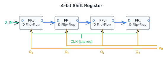
      • Write-after-read (WAR) or write-after-write (WAW) hazards (these arise in out-of-order execution, not covered).

      Summary of processor architectures

      ArchitectureCPIClock periodHardwareKey issue
      Single-cycle1LongRedundant (3 adders, 2 memories)Wastes time on fast instructions
      MulticycleVariable (~4)ShortReused (1 ALU, 1 memory)Complex FSM control
      Pipelined~1 (after fill)Short (per stage)Pipeline registers addedHazards

      See also:

  • Hardware Labs

    Overview of the hardware practical labs: breadboard prototyping, prototyping box features, gate-level (SSI), chip-level (MSI), and GAL-based implementations. Non-examinable practical content

    • Hardware Labs Overview

      The practical labs are non-examinable. You build and tick the circuits yourself in the Intel Lab during Michaelmas and Lent weeks, but the written Tripos paper does not test lab content. The notes below describe what you do and why, so the labs make sense, not so you can revise from them.

      What you do in the labs

      The hardware labs run alongside the lectures and put the lecture material into your hands. Over four workshops of 2.5 to 3 hours each, working individually at a bench in the Intel Lab (SW11 in the William Gates Building), you build and test small digital circuits. Each workshop ticks one piece of work and the labs continue through the Lent term.

      You progress through three implementation styles in roughly this order:

      • Gate-level (SSI): building combinational and sequential logic out of individual 74-series chips, where each chip holds a handful of gates or flip-flops.
      • Chip-level (MSI): using medium-scale integration parts such as counters and shift registers, which collapse a whole sub-circuit into one package.
      • GAL-based: programming a Generic Array Logic device (GAL) to implement an FSM by writing its next-state logic onto the AND plane.

      The point is to see how the same digital behaviour maps onto three different implementation technologies, and to learn the practical skills (reading pinouts, wiring cleanly, debugging) that lecture slides cannot convey.

      Lab implementation progression: SSI → MSI → GAL

      The prototyping box

      Each bench has a self-contained prototyping box with the building blocks you need:

      • a 5 V power supply (PSU) for the chips;
      • a clock generator producing a square wave you can use as the system clock;
      • push switches and logic switches (the latter give a stable 0 or 1 level rather than a momentary pulse);
      • LED displays for outputs and 7-segment displays for multi-bit values;
      • the breadboard itself in the centre where you plug in chips and wire them together.

      Prototyping box — PSU, clock generator, switches, breadboard, LEDs

      The breadboard

      The breadboard is what makes the labs reconfigurable. Two horizontal strips run along the top and bottom and are used to distribute Vcc (5 V) and GND (0 V) to the rest of the board. The main working area is a grid of vertical five-hole strips: any two pins in the same five-hole strip are connected internally, so you wire a circuit by plugging components into strips in the right pattern and bridging strips with jumper wire.

      Breadboard — horizontal power strips and vertical five-hole strips

      DIL packages and pin numbering

      The chips come in Dual In-Line (DIL) packages. A 14-pin DIL package for the 74HC00, for example, contains four 2-input NAND gates. The number tells you what you are looking at:
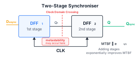
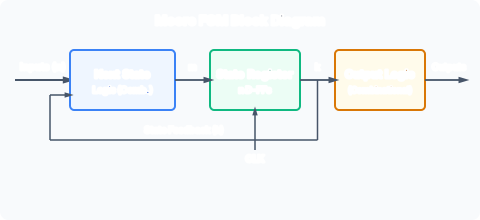
      • the prefix 74 is the series (the long-running 7400 logic family);
      • the HC identifies the technology (high-speed CMOS in this case);
      • the 00 identifies the function (quad 2-input NAND).
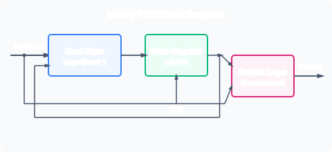
      Pin numbering is conventional. There is a small dot or notch at one end indicating pin 1. Numbering then proceeds anticlockwise when you look at the chip from above, going down the pin 1 side and back up the other side. As a rule, on a 14-pin package pin 7 is GND and pin 14 is Vcc; on a 16-pin package, pin 8 is GND and pin 16 is Vcc. There are exceptions, so check the datasheet, but when a circuit does not power up this is the first thing to verify.

      14-pin DIL package — 74HC00 quad NAND

      Building hints

      A few habits make the labs much less painful:

      • Draw a circuit diagram first. Write device IDs (IC1, IC2, …) on it and label which gate on a multi-gate package you are using (IC1a, IC1b). As you wire, cross off the connections in pencil so you do not miss one and so you can find mistakes by inspection.
      • Plan chip placement to minimise spaghetti. Place chips where their interconnect is short; debugging a rat’s nest of wire is miserable.
      • Wire power and ground first. Insert every chip with the same orientation (pin 1 to the left is conventional), check that no pins are bent under the body, then wire Vcc and GND to every chip. CMOS inputs are high impedance: if you leave them floating the gate can power up from its own input and you get random switching, high power draw and bizarre cross-talk on the same package.
      • Tie unused inputs to GND. Unused inputs on a CMOS gate are not “off”, they are antennas. Tie them to GND (or to the appropriate logic level) before powering up.
      • Do not wire over the top of a chip. You will need to reach pins to debug, and you will need to swap a chip if it dies. Wiring over the top blocks both.

      Testing hints

      When something does not work, debug systematically:

      1. Verify power. Using a digital multimeter (DMM) or an oscilloscope, confirm that every chip’s Vcc and GND pins are at the expected voltages. If every Vcc pin is at 0 V you almost certainly have a short between Vcc and GND.
      2. Verify the clock. Check the clock pin on any chip that needs one and confirm the frequency is what you think it is.
      3. Trace signal by signal. For a misbehaving gate or flip-flop, check the inputs first, then the output, then confirm that signal reaches the next input pin it should drive. A signal that is present at the output but missing at the next input is a wiring mistake; a signal at the input but wrong at the output is a bad chip.
      4. Look out for intermediate voltages. Outputs that are sitting somewhere between 0 V and 5 V (and not switching between them) almost always mean two outputs are shorted together, fighting each other.
      5. Throw away dead chips. If you identify a faulty IC, bin it rather than putting it back in the parts tray. Future you will thank past you.
      6. Ask a demonstrator. If you have a clear circuit diagram and a clean board and still cannot find the fault, by all means call for help. A demonstrator cannot do much with a messy board and no diagram, though, so the clean-diagram discipline pays off here too.

      Instruments

      Two main instruments are used:

      • The digital multimeter (DMM) measures DC voltage, current and resistance. It is the tool you will use most often, mainly to check power rails and logic levels at specific pins.
      • The oscilloscope (scope) displays voltage as a function of time and is essential for looking at clock signals, glitches and high-speed behaviour. Always make sure the probe’s ground clip is connected to the circuit GND; an ungrounded scope probe reads noise.

      Oscilloscope display — voltage vs time

      What the labs are for

      The lectures teach you what a flip-flop does on paper, what a state transition looks like in a state table and what an FSM is in the abstract. The labs teach you the unglamorous reality: that a real NAND gate has a propagation delay, that a breadboard connection can look fine and still be open, that floating CMOS inputs do silent damage, and that a defective IC is not a theory. After the labs the exam questions about setup/hold time, propagation delay and metastability read differently, because you have actually watched a clock edge arrive late on a scope.

      See also the GAL note which underpins one of the lab exercises:

      Generic Array Logic

  • Other Resources

    • Examinable Syllabus and Tripos Question Patterns

      Course overview

      • Course name: Digital Electronics
      • Paper: Part IA Paper 2, Questions 1 and 2 (typically Question 1 combinational logic, Question 2 sequential and electronics/processor)
      • Term: Michaelmas (lectures) with hardware labs running through Lent
      • Lecturer: Dr Ian Wassell
      • Format: Two questions on Paper 2; each worth 20 marks

      Examinable topics

      The course splits cleanly into the two Paper 2 questions. Question 1 is combinational logic; Question 2 is sequential logic, electronics and processor architecture. The lists below track the syllabus as delivered in the 2023 to 2026 lecture sets and cross-reference where each topic has been tested in the past.

      Combinational logic (Q1 territory)

      • Boolean algebra: identity, commutation, association, distribution, absorption, the consensus theorem; proving and simplifying expressions using these laws (and by expanding each term to include one instance of every variable).
      • DeMorgan’s theorem: rewriting expressions to switch between AND/OR forms; converting a circuit into NAND-only or NOR-only implementations using bubble logic.
      • Logic minimisation: truth tables, minterms and maxterms, disjunctive and conjunctive normal forms (DNF/CNF), sum-of-products and product-of-sums.
      • Karnaugh maps: 3- and 4-variable maps, SOP and POS simplification, don’t-care conditions, multiple equal-complexity minimal forms.
      • Quine-McCluskey method: tabular minimisation, prime implicants, cyclic covering tables, counting equal-complexity solutions.
      • Binary adders: half and full adder, ripple carry adder, carry generate/propagate/kill signals, carry lookahead.
      • Multilevel logic and hazards: common expression elimination, gate propagation delay, static-1/static-0 and dynamic hazards, hazard removal by adding a consensus term.
      • Beyond simple gates: multiplexers and demultiplexers, decoders, memories and ROMs, PLA and PAL, tristate buffers and bus contention. Multiplexer-only implementations of arbitrary Boolean functions are examined regularly (a function of nn inputs can be realised by a 2n:12^n{:}1 MUX with the function values on the data lines, or by smaller MUXes using variables as select signals).

      Frequently tested: Boolean algebra simplification, K-maps including don’t cares, Q-M with multiple equal solutions (2018 Q1, 2022 Q1, 2024 Q1), XOR identities and representing a function as the XOR of AND terms (2022 Q1, 2024 Q1, 2025 Q1), MUX implementation (2020 Q1).

      Sequential logic (Q2 territory)

      • Latches: cross-coupled NOR/NAND RS latch, truth table, state diagram, illegal condition.
      • Clocked and D-type devices: transparent D-latch (built from an RS latch and steering logic), master-slave D flip-flop (edge triggering from two latches in series), JK and T flip-flops, asynchronous preset and clear.
      • Flip-flop applications: ripple and synchronous counters, shift registers, serial links.
      • Timing: setup and hold time constraints, clock skew, metastability and resolution probability (the bounded-but-random settling time of a flip-flop driven into its metastable region). Calculation of maximum clock frequency from path delays, and of minimum operating period given setup/hold times.
      • Synchronous state machines: Moore versus Mealy, state diagrams and state tables, FSM design procedure, state assignment strategies (sequential, sliding, shift register, one-hot). Worked examples: traffic light controller and past Tripos FSMs.
      • State machine optimisation: row matching, state equivalence, the implication table.

      Frequently tested: D-FF next-state logic for counters with a mode input and self-start verification (2019 Q2, 2023 Q2, 2024 Q2), FSM state diagram and table from a problem description, state assignment and simplified D-input/output equations (2025 Q2, 2018 Q2), RS latch truth tables and D-latch construction from NOR gates (2017 Q2, 2018 Q2), state equivalence / implication table (2023 Q2, 2024 Q2), timing analysis of cascaded FF and combinational block paths with given setup/hold/propagation delays (2025 Q2).

      Electronics, transistors and CMOS (Q2)

      • Basic electricity: voltage, current, resistance, power, Ohm’s law (V=IRV = IR), Kirchhoff’s voltage and current laws, potential dividers.
      • Materials: insulators, conductors, silicon, doping to produce n-type and p-type semiconductors.
      • pn junction and diode: forward and reverse bias, threshold voltage.
      • MOSFET operation: n-channel and p-channel structure, gate controlling the drain-source current, characteristic curves of IDSI_{DS} against VDSV_{DS} for various VGSV_{GS}.
      • nMOS inverter with a resistor load: load line analysis on the MOSFET characteristics, finding VoutV_{out} for given VinV_{in}, calculating resistor value and power dissipation (the standard worked example with a lookup table of VDSV_{DS} and IDSI_{DS} values).
      • CMOS inverter and CMOS gates (NAND, NOR): transistor-level diagrams, sizing for symmetric switching, noise margin.
      • Logic families: voltage transfer characteristics, VOHV_{OH}, VOLV_{OL}, VIHV_{IH}, VILV_{IL}, noise margin NMHNM_H and NMLNM_L.

      Frequently tested: draw n-channel MOSFET structure and explain IDSI_{DS} control (2015 Q2, 2012 Q2), nMOS inverter circuit and load-line plot of VinV_{in} against VoutV_{out}, R and power calculation from a VDSV_{DS}/IDSI_{DS} table (2021 Q2, 2015 Q2, 2012 Q2). Examples paper 3 explicitly excludes rise and fall time calculations, so those are out of scope for Tripos revision.

      Processor architecture (Q2)

      • Architecture vs microarchitecture: the distinction between the architectural view (instructions, registers, programmer-visible state) and the microarchitectural view (datapath and control).
      • Simple computer: CPU, memory, buses.
      • Single-cycle processor: datapath including PC, instruction memory, register file, ALU, data memory and writeback; control signals per instruction type.
      • Modifying the single-cycle datapath to support data memory access instructions, and to support branching.
      • Multicycle processor: reusing the ALU and memory across cycles, microcoded control, CPI greater than 1.
      • Pipelined processor: pipeline stages IF/ID/EX/MEM/WB, throughput benefits versus single-cycle and multicycle.
      • Pipeline hazards: data hazards and control hazards; the names of solutions (stalling, forwarding, predict not-taken, branch delay slot) and the trade-offs at a conceptual level.

      Tested via examples paper 3 Q7 wording: “Explain the terms architecture and microarchitecture when applied to a processor. Show how the microarchitecture of a simple single cycle processor can be modified to permit data memory access / branching. What are the main advantages of a multicycle processor over a single cycle processor? How does a pipelined processor improve performance compared to a multicycle processor?” Past Paper 2 Tripos questions cited as relevant: 2023 Q2, 2021 Q2, 2019 Q2, 2015 Q2, 2012 Q2 (excluding rise and fall time calculations).

      Non-examinable material

      The following are part of the course but explicitly not tested in the written paper:

      • Hardware practical labs (breadboard prototyping, the prototyping box, SSI/MSI/GAL wiring exercises). Covered in Hardware Labs Overview.
      • HDL design flow beyond block-diagram level: synthesis, place and route and bitstream generation are taught conceptually, not examined at the level of vendor toolchains.
      • Detailed forwarding/stall logic, branch prediction algorithms and out-of-order hazards are reserved for the Part IB Computer Architecture course.
      • Rise and fall time calculations for CMOS (per Examples Paper 3 footnote).
      • FSM implementation technology specifics such as exact GAL device part numbers, Xilinx Spartan product families beyond the simplified CLB taught in lectures, or third-party FPGA tool features.

      Standard Q1 pattern (combinational logic)

      PartMarksTypeWhat to do
      (a)4 to 8Boolean algebraSimplify an expression into SOP or POS, prove an XOR identity, show a function equals XOR of AND terms
      (b)4 to 8Karnaugh mapSimplify a 4-variable function into SOP and/or POS, including don’t cares; identify multiple equal-complexity minimum forms
      (c)6 to 9Quine-McCluskeyReduce a function given as a sum of minterms; count the number of equal-complexity solutions
      (sometimes)6Multiplexer / decoderImplement a Boolean function using 8:1, 4:1, 2:1 MUXes with extra gates, or use a decoder as a building block

      Strategy:

      • For Boolean algebra, write the laws you apply (distribution, absorption, DeMorgan) as you go; markers reward method, not just the final expression.
      • For K-maps, label the axes clearly, draw the groups, and write the resulting product term next to each group. When asked for “multiple solutions” you must draw two groupings that yield different expressions of equal weight; do not just rearrange the same groups.
      • For Q-M, present the table of implicants by index (number of 1s) and chain merges carefully; tick off used implicants in the cover table and state explicitly when there are multiple equal-cost covers.

      Standard Q2 pattern (sequential, electronics, processor)

      Q2 is wider-ranging than Q1 and typically blends two or three of the sub-areas above. Common shapes seen across 2015 to 2025:

      Sequential-only Q2: design a counter with a mode input (state diagram, transition table, simplified D-input equations in SOP, self-start check), then design or reduce an FSM from a state table (state assignment, K-maps for next-state logic, sometimes implication-table state reduction).

      Mixed sequential and timing: build a flip-flop or counter, then add a setup/hold/propagation timing analysis of two cascaded flip-flops with combinational blocks between them (compute the maximum clock frequency and verify the hold-time constraint).

      Electronics-focused Q2: MOSFET characteristics, nMOS inverter circuit and load line, resistor value and power calculations from a VDSV_{DS}/IDSI_{DS} table.

      Processor Q2 (examples paper 3): architecture vs microarchitecture discussion, modify the single-cycle datapath for data memory or branching, advantages of multicycle over single-cycle, pipelining over multicycle. Past papers will reference 2012 Q2, 2015 Q2 and so on for these.

      Q2 partMarksTypeWhat to do
      (a)6 to 10Counter / latch / FF designState diagram, transition table, simplified SOP for D inputs, self-start verification
      (b)9 to 12FSM design or state reductionBuild or reduce an FSM, assign states, derive D-input and output equations; OR implication-table reduction with a reduced state table
      electronics12 to 14MOSFET and nMOS inverterStructure, IDSI_{DS} vs VDSV_{DS} curves, load line, R and power
      processor8 to 12Datapath / architectureModify single-cycle datapath, discuss multicycle and pipelining

      Strategy:

      • For counter design, always draw the state diagram and write the state transition table before K-mapping; this is where most marks hide.
      • For self-start questions, list every unused encoding and confirm it leads (possibly in several steps) into the main counting sequence. A single sentence “all unused states reach S0 in at most two transitions” with the explicit transitions shown earns the marks.
      • For implication-table questions, do row matching first even if not asked; it shrinks the table and makes the implication table faster to draw and check. Mark Xs in the table clearly and show at least one sweep pass so the marker can see the algorithm converging.
      • For timing analysis, write down the worst-case path delay formula (clock-to-Q + combinational delay + setup time) and only then substitute numbers; an algebraic answer that is numerically wrong still earns most of the marks.
      • For electronics, plot the load line by overlaying VRD=VDDIRV_{RD} = V_{DD} - I R on the MOSFET characteristics and report VoutV_{out} at both Vin=0V_{in} = 0 V and Vin=VDDV_{in} = V_{DD}. Power in the resistor uses P=I2RP = I^2 R or P=VRIP = V_R I; power in the transistor uses PMOS=VDSIDSP_{\text{MOS}} = V_{DS} I_{DS}.

      Past Paper 2 questions cited as relevant by the lecturer (Examples Papers 1 to 3):

      • Combinational logic (Examples Paper 1): Q1-2023, Q1-2022, Q1-2021, Q1-2020, Q1-2019, Q1-2018.
      • Sequential logic (Examples Paper 2): Q2-2023, Q2-2022, Q2-2020, Q2-2019, Q2-2018.
      • FSMs, electronics and processor (Examples Paper 3): Q2-2023, Q2-2021, Q2-2019, Q2-2015, Q2-2012 (excluding rise and fall time calculations).
      1. Boolean algebra and DeMorgan, then K-maps with don’t cares. These underpin every other part of Q1 and the next-state logic of Q2.
      2. Quine-McCluskey. Practice counting equal-cost solutions, since this is a near-annual sub-question.
      3. Latches and flip-flops, then counters and shift registers. Self-start questions and mode-input counters are mechanical once the state diagram habit is in place.
      4. FSM design and implication-table state reduction. The two skills (design up, reduce down) are tested together.
      5. Timing analysis (setup/hold, clock skew, metastability). One careful worked example is usually enough to internalise the algebra.
      6. Electronics and CMOS, last because it is rote-heavy: MOSFET operation, nMOS inverter load line, noise margin.
      7. Processor architecture at the conceptual level only: the comparison table of single-cycle, multicycle and pipelined architectures, plus the two requested modifications to the single-cycle datapath.

      Summary

      TopicQExaminable?Hard parts
      Boolean algebraQ1YesChoosing which law to apply; proving XOR identities
      Karnaugh maps (with don’t cares)Q1YesEqual-complexity minima are easy to miss
      Quine-McCluskeyQ1YesCounting equal-cost covers
      MUX/decoder implementationsQ1YesVariable-as-select tricks for smaller MUXes
      Hazards (static/dynamic)Q1YesThe consensus term to add when removing hazards
      Latches and flip-flopsQ2YesRS illegal condition, master-slave edge triggering
      Counters and shift registersQ2YesSelf-start verification
      FSM design + state reductionQ2YesImplication table sweeps
      Timing (setup/hold, metastability)Q2YesWorst-case path algebra
      Electronics and CMOSQ2YesLoad line, R and power from V/IV/I tables
      Processor architectureQ2Yes (conceptual)Single-cycle modifications, multicycle vs pipelined comparison
      Hardware labsEitherNoPractical only
      HDL flow specifics, vendor toolingQ2NoBeyond syllabus depth