Single-Cycle Processor
Design philosophy
In a single-cycle processor, every instruction executes completely in exactly one clock cycle. The control unit is purely combinational: the instruction opcode is decoded, all control signals are generated, and all datapath operations (register read, ALU, memory access, writeback) occur within that single cycle before the next rising clock edge.
The clock cycle must be long enough to accommodate the slowest instruction. This is the fundamental trade-off.
Datapath organisation
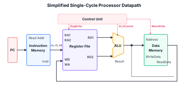
The single-cycle datapath contains:
- Instruction memory: a separate memory for instructions (Harvard architecture). Read-only in normal operation. Address comes from PC; output is the instruction word.
- Register file: two read ports (rs1, rs2), one write port (rd). Write happens on the clock edge.
- ALU: performs arithmetic/logical operations on two operands. One operand comes from register rs1; the other comes from either register rs2 or a sign-extended immediate (via the ALUsrc MUX).
- Data memory: a separate memory for data. Read or written depending on MemRead/MemWrite signals. Address comes from the ALU output. Write data comes from register rs2.
- PC logic: includes an adder for PC+1 (sequential), an adder for PC+branch-offset (branch target), and a MUX selecting between them.
- Multiplexers: at key points in the datapath to select between different data sources (register vs immediate for ALU, ALU result vs memory data for register writeback, PC+1 vs branch target for next PC).
Weaknesses
1. Clock cycle determined by slowest instruction
A LOAD instruction must: fetch from instruction memory, decode, read register file, compute address through ALU, read data memory, and write result to register file, all in one cycle. A simple ADD only needs: fetch, decode, read registers, ALU, writeback (no memory access). The LOAD sets the minimum clock period, yet for every ADD instruction, the ALU finishes long before the clock edge and then sits idle.
where T_LOAD > T_ADD, so T_clock = T_LOAD. All fast instructions waste time.
2. Redundant hardware
The single-cycle design requires:
- Three adders: one in the ALU (for arithmetic operations), one for PC+1 (incrementer), and one for PC+branch-offset (branch target adder).
- Two memories: separate instruction memory and data memory. This is a Harvard architecture, not the von Neumann shared-memory model. Both memories must be physically present, increasing cost.
3. All operations in parallel
Because everything happens in one cycle, all hardware units exist simultaneously. There is no reuse. A fast multibit adder is expensive (see carry lookahead design in the combinatory logic module). Having three of them is wasteful.
Execution time calculation
For N instructions, each taking exactly 1 clock cycle:
Compare this with a multicycle design where some instructions take fewer cycles: the trade-off is fewer cycles per simple instruction vs a shorter clock period overall.
Time per instruction = clocks per instruction (CPI) × clock period. Single-cycle: CPI = 1 always, but clock period is long. Multicycle: CPI > 1 but clock period is shorter. Pipelined: CPI approaches 1 but clock period is short (see /modules/digital-electronics/13-processor-architecture/06-pipelined-processor/).
Trace: LOAD instruction
Walk through the single-cycle execution of LOAD R1, [R2]:
- On the rising clock edge, the PC value is presented to the instruction memory’s address input.
- The instruction memory outputs
op=R2, rd=R1, rs2=R2combinatorially. - The register file reads R2: its value appears on the Read Data 2 output.
- The ALU receives R2 as operand A (from Read Data 1 or 2 depending on wiring) and computes the pass-through (effectively R2 + 0). The result is the memory address.
- The address is presented to the data memory. MemRead=1, so data memory outputs the value at that address.
- The MemtoReg MUX selects the data memory output, routing it to the register file’s write data input.
- RegWrite=1, and on the next rising clock edge, the value is written to R1.
- Simultaneously, the PC is updated to PC+1 (or branch target).
All of this happens between two rising clock edges.
Trace: BEQZ instruction
Walk through BEQZ R1, +10:
- Fetch instruction. Decode: BEQZ.
- Read R1 from register file.
- ALU computes R1 - 0. The zero flag is set if R1 = 0.
- The AND gate combines: (opcode == BEQZ) AND (zero_flag == 1). If both true, PCSrc = 1.
- The PC MUX selects: if PCSrc=1, the branch target (PC + 10) becomes the next PC. Otherwise, PC+1.
- No register writeback, no memory access.
The key: the branch decision and PC update all happen in the same cycle. The next instruction (at PC+1 or PC+10) is fetched on the next clock edge.
Diagrams
The course slides contain detailed datapath diagrams for the single-cycle processor, showing the progressive addition of components as more instructions are supported:
- Basic fetch: PC → instruction memory → adder → PC+1.
- Add register file and ALU for R-type instructions.
- Add data memory and result MUX for LOAD/STORE.
- Add branch target adder and PC MUX for BEQZ.
You should be able to sketch this datapath from memory, showing all the functional units and MUXes, and trace through each instruction type explaining which control signals are active.
See /modules/digital-electronics/13-processor-architecture/05-multicycle-processor/ for the next step: breaking the single cycle into multiple shorter cycles.