Shift Registers
What Is a Shift Register?
A shift register is a chain of D flip-flops where the output of each FF is connected to the D input of the next. On each clock edge, data shifts one position to the right (or left, depending on the wiring). Shift registers are fundamental building blocks for serial data communication, delay lines, and pattern generation.
Basic Structure (SISO/SIPO)
A 3-bit shift register with serial input Din and parallel outputs Q₀, Q₁, Q₂:
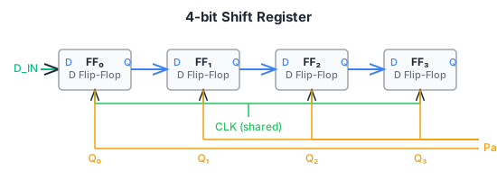
- D₀ = Din
- D₁ = Q₀
- D₂ = Q₁
On each clock edge:
- Q₀ ← Din
- Q₁ ← previous Q₀
- Q₂ ← previous Q₁
Worked Example: 4-bit SIPO Shift Register
Input sequence: 1, 0, 1, 1. All FFs initially 0.
| Clock | Din | Q₀ | Q₁ | Q₂ | Q₃ |
|---|---|---|---|---|---|
| 0 (init) | - | 0 | 0 | 0 | 0 |
| 1 | 1 | 1 | 0 | 0 | 0 |
| 2 | 0 | 0 | 1 | 0 | 0 |
| 3 | 1 | 1 | 0 | 1 | 0 |
| 4 | 1 | 1 | 1 | 0 | 1 |
| 5 | - | - | 1 | 1 | 0 |
After 4 clock edges, the 4-bit pattern 1011 has been shifted into the register (reading Q₃ downto Q₀: Q₃=1, Q₂=0, Q₁=1, Q₀=1). After 5 edges, the first bit (1) has been shifted out of Q₃.
This is SIPO (Serial-In, Parallel-Out): data enters serially and all Q outputs are available in parallel.
Four Configurations
Shift registers can be classified by their input/output configuration:
| Type | Input | Output | Application |
|---|---|---|---|
| SISO | Serial | Serial | Delay line (n-clock delay) |
| SIPO | Serial | Parallel | Serial-to-parallel conversion |
| PISO | Parallel | Serial | Parallel-to-serial conversion |
| PIPO | Parallel | Parallel | Register (load and hold) |
PISO (Parallel-In, Serial-Out): Uses asynchronous preset/clear inputs on each FF to load parallel data simultaneously (by asserting PRĒ/CLR̄ on each FF according to the data pattern). After loading, data is clocked out serially from the last FF.
SISO: The simplest configuration. After n clocks, Din appears at the output. A chain of n FFs produces a delay of n clock cycles. This is used for synchronising signals across clock domains.
Serial Data Link
Shift registers form the basis of serial communication:
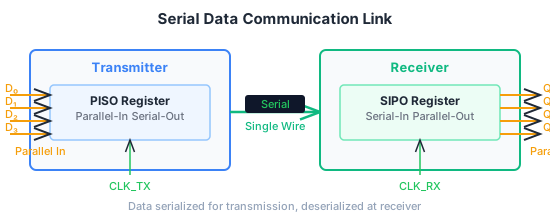
At the transmitter: a PISO register converts parallel data to a serial bit stream. At the receiver: a SIPO register converts the serial stream back to parallel data. Only one wire is needed for the data path (plus a shared clock or clock recovery mechanism), compared to n wires for a parallel link. This is how protocols like SPI, I²C, and UART operate at the physical level.
Feedback Shift Registers (LFSR)
If the serial input is derived from a function of the register outputs, the shift register becomes a sequence generator. The most common type is a Linear Feedback Shift Register (LFSR), which uses XOR gates to generate pseudo-random binary sequences.
Example: 3-stage LFSR with feedback from Q₁ ⊕ Q₂:
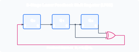
The feedback logic is D₀ = Q₁ ⊕ Q₂. Starting from 001 (Q₂=0, Q₁=0, Q₀=1):
| Clock | Q₀ | Q₁ | Q₂ | D₀ = Q₁⊕Q₂ |
|---|---|---|---|---|
| 0 | 1 | 0 | 0 | 0 |
| 1 | 0 | 1 | 0 | 1 |
| 2 | 1 | 0 | 1 | 1 |
| 3 | 1 | 1 | 0 | 1 |
| 4 | 1 | 1 | 1 | 0 |
| 5 | 0 | 1 | 1 | 0 |
| 6 | 0 | 0 | 1 | 1 |
| 7 | 1 | 0 | 0 | 0 → repeats |
The sequence length is 7 = 2³ - 1 states (excluding the all-zeros state, which would lock the register). This is a maximal-length LFSR. The choice of feedback taps (Q₁ and Q₂ for a 3-bit register, corresponding to the primitive polynomial x³ + x² + 1) determines the sequence length.
LFSRs are used for:
- Pseudo-random number generation in hardware
- CRC (Cyclic Redundancy Check) calculation for error detection
- Built-in self-test (BIST) for ICs
- Spread-spectrum communication
- Scrambling/descrambling in data transmission
Parallel Loading Shift Register
The asynchronous preset and clear inputs on each FF can be used to implement parallel loading. By connecting PRĒ to the desired parallel input bit (through appropriate gating), data can be loaded into all FFs simultaneously when a LOAD signal is asserted. After loading, normal shift operation proceeds. This is how PISO registers are built in practice.
Examples Paper Connection
The examples paper includes questions on shift registers with feedback. A typical question asks: given a shift register with specific feedback logic, determine the output sequence and the sequence length (period). The analysis is as shown above: trace through each clock cycle, compute the feedback value, and record the state until it repeats.