Hardware Labs Overview
The practical labs are non-examinable. You build and tick the circuits yourself in the Intel Lab during Michaelmas and Lent weeks, but the written Tripos paper does not test lab content. The notes below describe what you do and why, so the labs make sense, not so you can revise from them.
What you do in the labs
The hardware labs run alongside the lectures and put the lecture material into your hands. Over four workshops of 2.5 to 3 hours each, working individually at a bench in the Intel Lab (SW11 in the William Gates Building), you build and test small digital circuits. Each workshop ticks one piece of work and the labs continue through the Lent term.
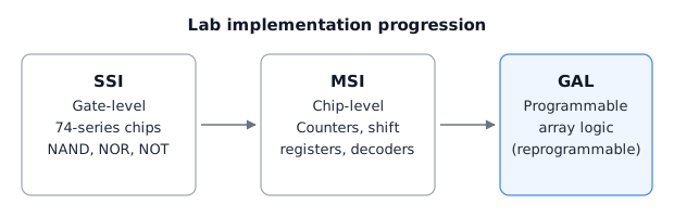
You progress through three implementation styles in roughly this order:
- Gate-level (SSI): building combinational and sequential logic out of individual 74-series chips, where each chip holds a handful of gates or flip-flops.
- Chip-level (MSI): using medium-scale integration parts such as counters and shift registers, which collapse a whole sub-circuit into one package.
- GAL-based: programming a Generic Array Logic device (GAL) to implement an FSM by writing its next-state logic onto the AND plane.
The point is to see how the same digital behaviour maps onto three different implementation technologies, and to learn the practical skills (reading pinouts, wiring cleanly, debugging) that lecture slides cannot convey.
The prototyping box
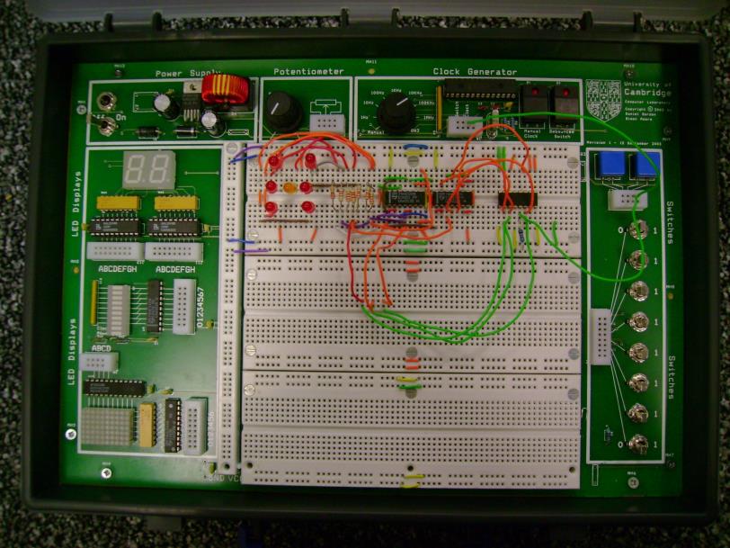
Each bench has a self-contained prototyping box with the building blocks you need:
- a 5 V power supply (PSU) for the chips;
- a clock generator producing a square wave you can use as the system clock;
- push switches and logic switches (the latter give a stable 0 or 1 level rather than a momentary pulse);
- LED displays for outputs and 7-segment displays for multi-bit values;
- the breadboard itself in the centre where you plug in chips and wire them together.
The breadboard
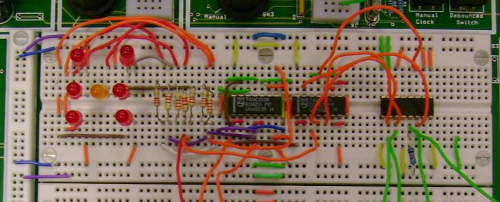
The breadboard is what makes the labs reconfigurable. Two horizontal strips run along the top and bottom and are used to distribute Vcc (5 V) and GND (0 V) to the rest of the board. The main working area is a grid of vertical five-hole strips: any two pins in the same five-hole strip are connected internally, so you wire a circuit by plugging components into strips in the right pattern and bridging strips with jumper wire.
DIL packages and pin numbering
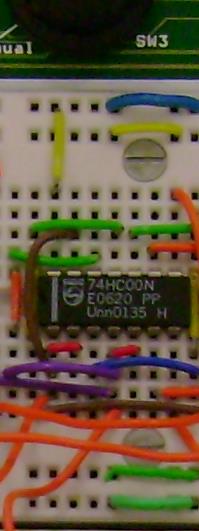
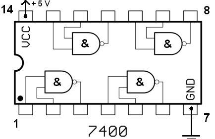
The chips come in Dual In-Line (DIL) packages. A 14-pin DIL package for the 74HC00, for example, contains four 2-input NAND gates. The number tells you what you are looking at:
- the prefix
74is the series (the long-running 7400 logic family); - the
HCidentifies the technology (high-speed CMOS in this case); - the
00identifies the function (quad 2-input NAND).
Pin numbering is conventional. There is a small dot or notch at one end indicating pin 1. Numbering then proceeds anticlockwise when you look at the chip from above, going down the pin 1 side and back up the other side. As a rule, on a 14-pin package pin 7 is GND and pin 14 is Vcc; on a 16-pin package, pin 8 is GND and pin 16 is Vcc. There are exceptions, so check the datasheet, but when a circuit does not power up this is the first thing to verify.
Building hints
A few habits make the labs much less painful:
- Draw a circuit diagram first. Write device IDs (IC1, IC2, …) on it and label which gate on a multi-gate package you are using (IC1a, IC1b). As you wire, cross off the connections in pencil so you do not miss one and so you can find mistakes by inspection.
- Plan chip placement to minimise spaghetti. Place chips where their interconnect is short; debugging a rat’s nest of wire is miserable.
- Wire power and ground first. Insert every chip with the same orientation (pin 1 to the left is conventional), check that no pins are bent under the body, then wire Vcc and GND to every chip. CMOS inputs are high impedance: if you leave them floating the gate can power up from its own input and you get random switching, high power draw and bizarre cross-talk on the same package.
- Tie unused inputs to GND. Unused inputs on a CMOS gate are not “off”, they are antennas. Tie them to GND (or to the appropriate logic level) before powering up.
- Do not wire over the top of a chip. You will need to reach pins to debug, and you will need to swap a chip if it dies. Wiring over the top blocks both.
Testing hints
When something does not work, debug systematically:
- Verify power. Using a digital multimeter (DMM) or an oscilloscope, confirm that every chip’s Vcc and GND pins are at the expected voltages. If every Vcc pin is at 0 V you almost certainly have a short between Vcc and GND.
- Verify the clock. Check the clock pin on any chip that needs one and confirm the frequency is what you think it is.
- Trace signal by signal. For a misbehaving gate or flip-flop, check the inputs first, then the output, then confirm that signal reaches the next input pin it should drive. A signal that is present at the output but missing at the next input is a wiring mistake; a signal at the input but wrong at the output is a bad chip.
- Look out for intermediate voltages. Outputs that are sitting somewhere between 0 V and 5 V (and not switching between them) almost always mean two outputs are shorted together, fighting each other.
- Throw away dead chips. If you identify a faulty IC, bin it rather than putting it back in the parts tray. Future you will thank past you.
- Ask a demonstrator. If you have a clear circuit diagram and a clean board and still cannot find the fault, by all means call for help. A demonstrator cannot do much with a messy board and no diagram, though, so the clean-diagram discipline pays off here too.
Instruments
Two main instruments are used:
- The digital multimeter (DMM) measures DC voltage, current and resistance. It is the tool you will use most often, mainly to check power rails and logic levels at specific pins.
- The oscilloscope (scope) displays voltage as a function of time and is essential for looking at clock signals, glitches and high-speed behaviour. Always make sure the probe’s ground clip is connected to the circuit GND; an ungrounded scope probe reads noise.
What the labs are for
The lectures teach you what a flip-flop does on paper, what a state transition looks like in a state table and what an FSM is in the abstract. The labs teach you the unglamorous reality: that a real NAND gate has a propagation delay, that a breadboard connection can look fine and still be open, that floating CMOS inputs do silent damage, and that a defective IC is not a theory. After the labs the exam questions about setup/hold time, propagation delay and metastability read differently, because you have actually watched a clock edge arrive late on a scope.
See also the GAL note which underpins one of the lab exercises: