Generic Array Logic (GAL)
From PLA to programmable sequential logic
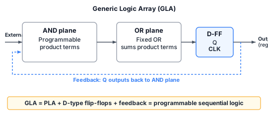
The Programmable Logic Array devices you met earlier are purely combinational: an AND plane feeds an OR plane, and that is the end of the story. To make a finite state machine you would have to wire D-type flip-flops around the PLA by hand on a separate board, which is fiddly and defeats the point of programmable logic.
A Generic Logic Array (GLA) solves this by integrating the flip-flops onto the same chip. The structure is the same as a PLA (AND plane into OR plane) but each OR gate is followed by a D-type flip-flop. The Q outputs of those flip-flops are then fed back into the AND plane alongside the external inputs. The chip is now able to implement sequential circuits, because its outputs depend on its stored state as well as on the inputs.
From GLA to GAL
A GLA is a useful building block but the AND and OR planes are programmed at the factory, which makes it expensive to change. A Generic Array Logic (GAL) device is the reprogrammable version of the GLA: the AND and OR plane connections are stored in reconfigurable memory (typically E²CMOS, which is electrically erasable), so the same physical chip can be programmed and reprogrammed many times.
A GAL therefore offers:
- the AND plane / OR plane / D-FF structure of a GLA, in one package;
- a fixed OR plane and programmable AND plane (the PAL inheritance);
- D-FF outputs fed back into the AND plane, making sequential circuits first-class;
- reprogrammability, so you can experiment in the lab without burning new silicon.
This is the device family used in the Digital Electronics hardware labs to implement FSMs. You write a state table, work out the next-state and output logic for each D-FF input, then map the Boolean expressions onto the AND plane. Each product term corresponds to one row of the AND plane, and the OR plane combines the product terms needed for each flip-flop input.
An output structure worth noting
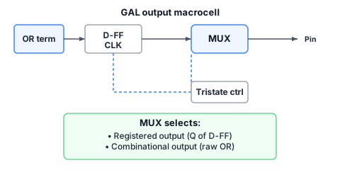
The GAL output cell is more than just “feed the OR gate into a D-FF”. The cell typically includes a multiplexer that lets you choose whether the pin presents:
- the registered output (the Q of the D-FF), for synchronous behaviour, or
- the combinational output (the raw OR gate result), when you only need combinational logic on that pin.
There is also an output-enable control, which lets the pin be tristated so that it can drive a shared bus without contention. The reason this is on the syllabus rather than a different chip family is that these output cells are what gives the GAL its flexibility: a single device can act as a shift register, a counter, a Mealy or Moore FSM controller, or a chunk of combinational glue logic between other chips.
Limitations of GALs
GALs cover the small-scale FSM needs of the labs, but they run out of room quickly for anything serious:
- The AND plane grows as where is the number of inputs (external inputs plus feedback), so the device hits a ceiling at around a dozen or so input lines.
- The OR plane on a PAL/GAL is fixed, meaning each OR gate has a hard limit on how many product terms it can sum.
- The number of D-FFs is fixed by the package pin count and output cells, so large unrolled state machines cannot fit.
For bigger designs, you switch to a fundamentally different programmable architecture, the FPGA: