PLA and PAL Structures
Programmable logic
Standard SSI/MSI gates are fixed-function devices. Programmable logic devices (PLDs) allow the user to define custom logic functions by programming connections (fuses, anti-fuses, or SRAM cells) inside the chip. The two classic architectures are PLA and PAL.
PLA (Programmable Logic Array)
A PLA has two programmable planes: both the AND plane and the OR plane are programmable.
Structure:
- Inputs (true and complemented) feed the AND plane.
- The AND plane computes user-defined product terms. Any AND gate can connect to any input (or none).
- The OR plane sums (ORs) the product terms. Any OR gate can connect to any product term from the AND plane.
- Outputs may optionally go through a flip-flop for registered operation.
Both planes are programmed. A PLA can implement multiple Boolean functions that share product terms, which is its key advantage: if two functions use the same product term, it is computed once in the AND plane and reused in the OR plane.
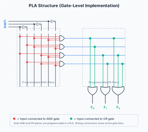
PLA example
Implement f1 = a·b + b̄·c and f2 = a·b + a·c using a PLA.
Product terms needed: a · b, b̄ · c, a · c.
The AND plane: three AND gates compute these three product terms.
The OR plane: f1 connects to terms 1 and 2; f2 connects to terms 1 and 3.
Notice that a·b is shared between both outputs, saving one AND gate compared to implementing each function independently.
PAL (Programmable Array Logic)
A PAL has a programmable AND plane but a fixed OR plane. Each OR gate has a predetermined number of AND gate inputs feeding it (typically 7-8). This makes PALs simpler, faster, and cheaper than PLAs, at the cost of flexibility: each output is limited to a fixed number of product terms.
The AND plane is programmed: the user decides which inputs (true or complemented) connect to each AND gate, creating the desired product terms. The OR connections are permanently wired.
PAL vs PLA comparison
| Feature | PLA | PAL |
|---|---|---|
| AND plane | Programmable | Programmable |
| OR plane | Programmable | Fixed |
| Flexibility | High (share all terms) | Moderate (fixed OR connections) |
| Speed | Slower (two programmable planes) | Faster (one programmable plane) |
| Cost | Higher | Lower |
| Use case | Complex multi-output logic with shared terms | Simpler glue logic, state machine implementation |
GAL (Generic Array Logic)
A GAL is an erasable, reprogrammable PAL. The key innovation: an EEPROM-based AND plane that can be erased and reprogrammed multiple times, unlike one-time-programmable PALs. This is the device used in the Cambridge hardware labs.
GALs also feature Output Logic Macrocells (OLMCs) that can configure each output pin as:
- Combinational output (registered or directly from OR gate).
- Combinational I/O (bidirectional, with output enable control).
- Registered output (OR gate feeds a D flip-flop, then the pin).
- Input only (pin bypasses the logic array entirely).
The OLMC makes GALs suitable for implementing both combinational logic and simple FSMs. The GAL programming flow in labs: write HDL → compile → generate JEDEC file → program GAL → test on breadboard. The JEDEC file specifies which fuses to blow in the AND plane.
Evolution
Modern programmable logic has evolved from PAL/GAL to CPLDs (complex PLDs — multiple PAL-like blocks interconnected) and FPGAs (field-programmable gate arrays — fine-grained LUT-based logic with programmable routing), covered in the FSM implementation technologies notes. All share the same fundamental idea: a programmable AND/OR or LUT structure, configured by the designer to implement arbitrary logic.