Tristate Buffers and Bus Contention
The tristate buffer
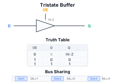
A standard logic gate always actively drives its output to either logic 0 or logic 1. A tristate buffer adds a third state: high-impedance (Z), in which the output is effectively disconnected from the circuit. This is controlled by an Output Enable (OE) input.
| OE | Data In | Output |
|---|---|---|
| 0 | X | Hi-Z (disconnected) |
| 1 | 0 | 0 |
| 1 | 1 | 1 |
When OE = 0, the buffer presents a very high resistance to the output line; it neither sources nor sinks current. When OE = 1, it acts as a normal buffer.
Symbol: a triangle (buffer) with an enable input on the side (or top/bottom). Active-low enable is often marked with a bubble.
Motivation: shared buses
In a system with multiple devices (CPU, memory, I/O peripherals) connected to a common data bus, only one device should drive the bus at any given time. If two devices drive simultaneously with opposite values, the result is bus contention: the two outputs fight each other, causing excessive current flow, potential damage, and undefined logic levels.
The solution: every device that can drive the bus does so through a tristate buffer. The system ensures that at most one buffer is enabled at any time; all others are in Hi-Z state.
Bus contention analysis
Consider two tristate buffers driving the same bus line. If both are enabled simultaneously:
- If one drives 1 and the other 0: a low-impedance path exists from VDD to ground through both transistors. Large current flows → potential damage, voltage at an indeterminate level between 0 and VDD.
- If both drive the same value: technically safe but still wasteful (two drivers fighting with minor voltage differences).
The control logic must guarantee mutual exclusion: only one OE at a time is asserted. This is typically done by a decoder that enables exactly one device for a given address range (memory address decoding) or by a bus arbiter that grants access to one requestor at a time.
Tristate buffer implementation
At the transistor level, a tristate buffer in CMOS uses a transmission gate or an extra pair of transistors that can disconnect both the pull-up and pull-down paths when OE is de-asserted. In n-MOS or TTL, the mechanism is different but the external behaviour is the same: three possible output states.
Multiplexer vs tristate bus
A multiplexer also routes one of several data sources to a destination. Comparison:
| Aspect | MUX | Tristate bus |
|---|---|---|
| Implementation | Logic gates (AND-OR) | Tristate drivers + shared wire |
| Number of wires | Each source needs dedicated wire to MUX | All share one bus wire |
| Contention risk | Inherently safe | Must guarantee mutual exclusion |
| Speed | Gate delay through MUX | Wire delay + buffer delay |
| Scalability | Adding sources increases MUX size | Just add another driver to bus |
| Use case | On-chip logic selection | Board-level buses, backplanes |
Modern on-chip designs favour MUXes because contention avoidance is free (guaranteed by construction) and wires are cheap inside a chip. Board-level designs use tristate buses because they dramatically reduce the number of physical wires.
Control signals
The OE signals are generated by a control unit or address decoder. For a memory-mapped I/O system: the address bus partially feeds a decoder, and each decoder output becomes the OE for one device’s data bus tristate buffer. During a memory read cycle, exactly one device is selected.
Real-world examples
- PCI/PCIe bus: multiple cards share address/data lines with tristate or differential drivers.
- Microcontroller GPIO: pins can be configured as input (Hi-Z), output (driven 0 or 1), or peripheral function.
- FPGA I/O: every output pin has a tristate buffer controlled by the design’s logic.
- Memory data bus: SRAM/DRAM data outputs are tristate; the processor’s memory controller enables one chip’s output during a read cycle.
The tristate concept is fundamental to bus-based architectures and is essential for understanding how multiple devices share a common communication medium.