Memory Elements and the RS Latch
The Shift from Combinational to Sequential Logic
All circuits studied so far have been combinational: the output depends only on the current inputs. Such circuits have no notion of history; they compute a function and that is all. Sequential logic introduces memory: the output depends not only on the current inputs, but also on previous inputs. The key mechanism that enables memory is feedback: feeding an output signal back to an input.
A bistable is a circuit with two stable internal states. Flip-flops and latches are particular implementations of bistables. The simplest memory element is the RS latch (Reset-Set latch).
The NOR-Based RS Latch
The RS latch consists of two cross-coupled NOR gates:
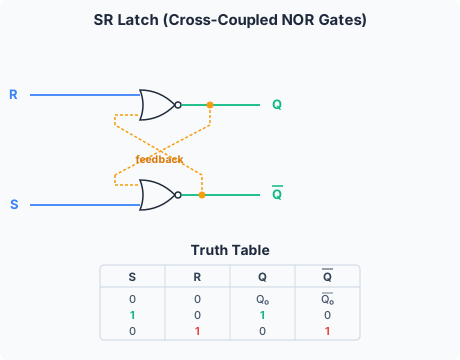
Gate 1 takes inputs R and Q (the output of Gate 2). Gate 2 takes inputs S and Q (the output of Gate 1). Recall the NOR truth table:
| a | b | a NOR b |
|---|---|---|
| 0 | 0 | 1 |
| 0 | 1 | 0 |
| 1 | 0 | 0 |
| 1 | 1 | 0 |
From this table, observe two special cases:
- If one input is 0, the NOR acts as an inverter on the other input (the “complement” condition, since 0 NOR b = b̄).
- If one input is 1, the output is always 0 (the “always 0” condition, since 1 NOR b = 0 regardless of b).
These two observations are the key to understanding latch behaviour.
Step-by-Step Behaviour: All Four Input Combinations
1. Reset: R = 1, S = 0
Gate 1 sees R = 1, so it is in the “always 0” condition: Q = 0. Gate 2 sees S = 0 and Q = 0 (the feedback from Gate 1), so it is in the “complement” condition: Q̄ = 1. This is the reset condition: Q is forced to 0.
2. Hold (following Reset): R = 0, S = 0
After the reset, we change R from 1 to 0. Gate 1 now sees R = 0 and Q̄ = 1 (from Gate 2), placing it in the “complement” condition: Q = 0 (unchanged!). Gate 2 sees S = 0 and Q = 0, remaining in the “complement” condition: Q̄ = 1. The latch holds its previous state. This is the memory behaviour: with both inputs at 0, the latch retains whatever state it was last in.
3. Set: R = 0, S = 1
Gate 2 sees S = 1, placing it in the “always 0” condition: Q̄ = 0. Gate 1 sees R = 0 and Q̄ = 0, placing it in the “complement” condition: Q = 1. This is the set condition: Q is forced to 1. Going back to R = S = 0 now holds Q = 1.
4. Forbidden: R = 1, S = 1
Both gates are in the “always 0” condition: Q = 0 and Q̄ = 0. This breaks the fundamental invariant of the latch: Q and Q̄ should always be complements. The condition is called illegal or forbidden. Worse, if both inputs are simultaneously returned to 0, the subsequent state is unpredictable. If Gate 1 is slightly faster than Gate 2, both outputs might go to 1 momentarily, causing an oscillation or an indeterminate settling point. This is a race condition: the outcome depends on which gate’s propagation delay is shorter.
State Transition Table
The state transition table shows, for each combination of current state Q and inputs R, S, what the next state Q’ will be:
| Q | S | R | Q’ | Comment |
|---|---|---|---|---|
| 0 | 0 | 0 | 0 | Hold |
| 0 | 0 | 1 | 0 | Reset (already 0) |
| 0 | 1 | 0 | 1 | Set |
| 0 | 1 | 1 | 0 | Illegal |
| 1 | 0 | 0 | 1 | Hold |
| 1 | 0 | 1 | 0 | Reset |
| 1 | 1 | 0 | 1 | Set (already 1) |
| 1 | 1 | 1 | 0 | Illegal |
State Diagram
The RS latch has two states: Q = 0 and Q = 1. The state diagram shows the input conditions for each transition:
- To remain in Q = 0: S̄ + R̄ (i.e., not S and R both 0, or R = 1). More simply: stay in Q = 0 if S̄ + R̄. From the table, the transitions Q = 0 to Q’ = 0 occur when S·R̄ + S̄·R̄ + S̄·R = S̄(R̄ + R) + S̄·R = S̄ + S̄·R = (S + S̄)(S̄ + R) = S̄ + R. So the self-loop on Q = 0 is labelled S̄ + R.
- To transition from Q = 0 to Q = 1: S · R̄ (set condition).
- To remain in Q = 1: R̄ (from S̄·R̄ + S·R̄ = R̄(S̄ + S) = R̄).
- To transition from Q = 1 to Q = 0: R (reset condition).
The resulting state diagram has two circles (Q = 0 and Q = 1) with these transition arcs labelled.
Asynchronous Nature
The RS latch is asynchronous: outputs change immediately in response to input changes, with only the propagation delays of the NOR gates (typically nanoseconds) determining response time. There is no clock signal. While simple, this asynchronous behaviour causes problems in larger designs because:
- Input glitches can cause spurious state changes.
- Timing is unpredictable: different paths through the circuit have different delays.
- It is difficult to reason about the behaviour of many interacting asynchronous latches.
The NAND-Based RS Latch Variant
An RS latch can also be built from two cross-coupled NAND gates. The NAND variant has active-low inputs, typically denoted S̄ and R̄. The behaviour is:
- S̄ = 1, R̄ = 1: hold (both inputs inactive)
- S̄ = 0, R̄ = 1: set (Q = 1)
- S̄ = 1, R̄ = 0: reset (Q = 0)
- S̄ = 0, R̄ = 0: forbidden (Q = Q̄ = 1)
The active-low nature follows from the NAND truth table: NAND with one input at 1 acts as an inverter on the other; with one input at 0, output is always 1. The analysis is symmetric to the NOR case but with the roles of 0 and 1 swapped.
Practical Significance
The RS latch demonstrates the fundamental principle of memory through feedback. It is the foundation upon which all clocked storage elements are built. The forbidden state problem motivates the D latch (covered in the next note), which uses a single data input and an enable signal to prevent the illegal R = S = 1 condition by construction.