Clocks and Synchronous Circuits
The Problem with Asynchronous Design
The RS latch described previously is asynchronous: its output changes immediately in response to input changes. In a complex digital system, this creates several serious problems:
Glitch sensitivity. Combinational logic produces glitches (transient incorrect outputs) while signals propagate through different paths. If such a glitch reaches an asynchronous latch’s input, it can cause a spurious state change. The latch has no way to distinguish a glitch from a genuine signal.
Unpredictable timing. Different signal paths have different propagation delays. With asynchronous elements, the order in which state changes occur is determined by these delays, which vary with temperature, supply voltage, and manufacturing process. Designing a large asynchronous system that works correctly under all conditions is extremely difficult.
Hard to reason about at scale. When multiple asynchronous latches interact, the number of possible timing scenarios explodes. Verification becomes intractable. Most practical digital systems use synchronous design to avoid this complexity.
The Clock: A Periodic Timing Reference
The solution is a clock: a periodic square wave signal distributed throughout the circuit. State changes in sequential elements are constrained to occur only at specific moments defined by the clock.
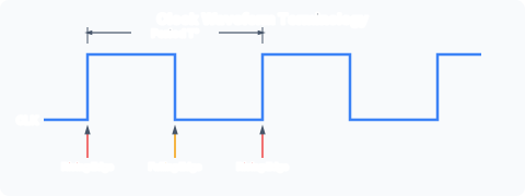
Clock waveform terminology:
- Period (Tc): the time between successive rising edges (or between successive falling edges). Measured in seconds.
- Frequency (f = 1/Tc): the number of clock cycles per second, measured in Hertz (Hz). Modern processors operate at several GHz.
- Duty cycle: the fraction of the period for which the clock is high. A perfect square wave has a 50% duty cycle.
- Rising edge (positive edge): the transition from low to high.
- Falling edge (negative edge): the transition from high to low.
A typical clock waveform:
Level-Sensitive vs Edge-Triggered
Sequential elements respond to the clock in one of two ways:
Level-sensitive (transparent) devices pass data through while the clock is in a particular state. A D latch, for example, is transparent when EN = 1 and holds when EN = 0. The output can change at any time during the active level: if the data input changes while the clock is high, the output follows.
Edge-triggered devices sample the data input only at the moment of a clock edge. At all other times, the output is held stable. The D flip-flop samples D on the rising edge of the clock. Once the sample is taken, changes to D have no effect until the next rising edge.
The edge-triggered behaviour is preferred for synchronous design because it introduces a clean abstraction: the state of the entire system is captured at a single instant (the clock edge), and combinational logic can compute the next state during the remainder of the clock period.
Why Synchronous Design Dominates
Synchronous design imposes a discipline that simplifies design enormously:
-
Predictable timing. The designer only needs to ensure that signals propagate through combinational logic fast enough to meet the setup time of the next sequential element before the next clock edge. A single global constraint replaces analysis of all possible asynchronous interaction patterns.
-
Easier verification. The state of the system is well-defined at clock edges. Functional verification can proceed one clock cycle at a time, treating the combinational logic as a pure function. This is the foundation of finite state machine (FSM) design.
-
Pipelining. By inserting registers between stages of combinational logic, a synchronous design can overlap the execution of different operations. Stage 1 processes data A while stage 2 processes the result of data A from the previous cycle. Pipelining dramatically increases throughput with only modest hardware cost.
-
Glitch immunity. Since outputs are sampled only at clock edges, glitches in combinational logic are harmless as long as they have settled by the time the next edge arrives. This eliminates the need for glitch-free design at every gate.
Setting the Stage
The synchronous methodology depends on two fundamental building blocks: the transparent D latch (level-sensitive, used as a component of flip-flops) and the edge-triggered D flip-flop (the workhorse of synchronous design). The next two notes develop these in detail.
Clock Distribution
In a real system, the clock signal must be distributed to thousands or millions of sequential elements. Wire delays mean the clock edge does not arrive at all elements simultaneously: this variation is called clock skew, and it has serious timing implications discussed later in /modules/digital-electronics/07-flip-flop-applications-and-timing/05-clock-skew/. Clock distribution networks (H-trees, grids) are designed to minimise skew at the cost of silicon area and power.