Transparent D Latch
From RS Latch to D Latch
The RS latch has a fundamental problem: the R = S = 1 forbidden state, which breaks the Q = Q̄ invariant and can cause unpredictable behaviour if both inputs return to 0 simultaneously. The D latch (Data latch) solves this by adding gating logic that ensures exactly one of R and S is active at any time, and both are inactive when the latch is disabled.
Structure
The D latch is built by adding two AND gates in front of the RS latch’s inputs, controlled by an enable (EN) signal:
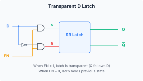
The data input D is connected to S through an AND gate: S = D · EN. The complement D̄ is connected to R through another AND gate: R = D̄ · EN. (In practice, a single inverter generates D̄ from D.)
When EN = 0, both AND gate outputs are 0, so R = S = 0: the RS latch holds its state. When EN = 1, exactly one of D or D̄ is 1, so exactly one of R or S is 1:
- If D = 1: S = 1 · 1 = 1, R = 0 · 1 = 0 → latch is set, Q = 1.
- If D = 0: S = 0 · 1 = 0, R = 1 · 1 = 1 → latch is reset, Q = 0.
The forbidden R = S = 1 condition is eliminated by construction: it is impossible for both D and D̄ to be 1 simultaneously.
Truth Table
| EN | D | Q’ | Q̄’ | Comment |
|---|---|---|---|---|
| 0 | X | Q | Q̄ | Hold (latch disabled) |
| 1 | 0 | 0 | 1 | Output follows D |
| 1 | 1 | 1 | 0 | Output follows D |
Where X means “don’t care”: when EN = 0, D has no effect.
The Transparency Property
The D latch is called transparent because when EN = 1, Q follows D directly (after a short propagation delay). Any change to D while EN remains 1 immediately propagates to Q. When EN drops to 0, Q freezes at the last sampled value of D.
This is both the D latch’s strength and its weakness. The ability to pass data through when enabled is useful for certain applications (such as bus holding registers). But for clocked synchronous systems, the transparency creates a problem: if the latch is enabled for a whole clock half-period, the data input might change during that time, propagating multiple transitions to the output. This violates the discipline that state should change at most once per clock cycle.
Timing Diagram

When EN = 1, Q tracks D after the latch’s propagation delay. When EN = 0, Q holds its last value regardless of changes to D. Note that a glitch on D while EN = 1 would propagate to Q: the latch does not filter glitches.
The Latch as a Building Block
The D latch is not typically used directly in clocked designs. Instead, it serves as the building block for the master-slave D flip-flop, which solves the transparency problem by combining two latches operating on opposite clock phases. The result is an edge-triggered device that samples D only at a specific clock edge, discussed in /modules/digital-electronics/06-latches-and-flip-flops/04-master-slave-d-flip-flop/.
Comparison with the RS Latch
| Property | RS Latch | D Latch |
|---|---|---|
| Inputs | R, S (two) | D, EN (two) |
| Forbidden state? | Yes (R = S = 1) | No |
| Memory behaviour | When R = S = 0 | When EN = 0 |
| Active condition | Always responds to inputs | Only when EN = 1 |
| Complement outputs? | Q and Q̄ | Q and Q̄ (from internal RS latch) |
The D latch eliminates the forbidden state and adds gating control at the cost of one inverter and two AND gates. It is the simplest practical clocked storage element.