Master-Slave D Flip-Flop
The Transparency Problem
The transparent D latch passes data through whenever EN = 1. In a clocked system where EN is the clock signal, the latch would be transparent for the entire half-period when CLK = 1. Any change to D during this time would propagate to Q. This breaks the synchronous design discipline: we want each storage element to change state at most once per clock cycle, at a well-defined instant.
The master-slave D flip-flop solves this by cascading two D latches that operate on opposite clock phases.
Structure
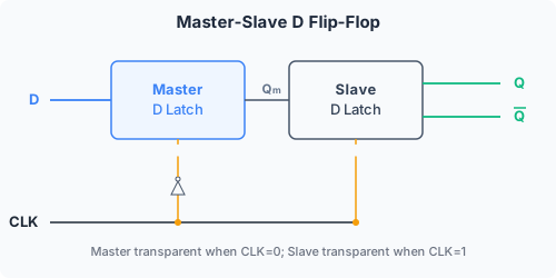
Two D latches are connected in series:
- The master latch has its enable connected to CLK̄ (the complement of the clock). It is transparent when CLK = 0.
- The slave latch has its enable connected to CLK. It is transparent when CLK = 1.
- The output of the master (Q_int, the internal signal) is connected to the D input of the slave.
- The output of the slave is the flip-flop’s Q output.
Operation Through a Clock Cycle
Trace the behaviour step by step through a full clock cycle:
Phase 1: CLK = 0. The master latch is transparent (EN = 1), so Q_int follows D. The slave latch is disabled (EN = 0), so Q holds its previous value. D is being loaded into the master while the output remains stable.
Phase 2: CLK rises (0 → 1). The master latch is disabled (EN = 0), freezing Q_int at the last value of D before the rising edge. The slave latch becomes transparent (EN = 1), so Q follows Q_int. After the slave’s propagation delay, Q takes the value that D had at the rising edge.
Phase 3: CLK = 1. The master remains disabled. Changes to D have no effect on Q_int. The slave remains transparent, but Q_int is stable (held by the master), so Q is stable. D can change freely without affecting the output: this is the desired edge-triggered behaviour.
Phase 4: CLK falls (1 → 0). The slave is disabled, freezing Q. The master becomes transparent, beginning to load the next value of D. The cycle repeats.
The net result: D is sampled on the rising edge of CLK. The output Q changes a short time (the slave’s propagation delay) after the rising edge, and remains stable for the rest of the cycle.
Timing Diagram
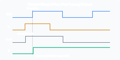
At the rising edge of CLK, the master freezes Q_int at the last value of D. After the slave’s propagation delay, Q reflects Q_int. Q then holds stable until the next rising edge, regardless of subsequent changes to D.
The 1s Catching Problem
The master-slave structure has a subtle flaw. During CLK = 1, the master is disabled but the slave is transparent. If a narrow pulse on D occurs while CLK = 1, could it affect the output? No: the master is frozen, so Q_int cannot change. The master-slave D flip-flop does not have a “1s catching” problem for pulses on D during CLK = 1.
However, there is a related issue: if D changes right as the clock rises (violating setup/hold time), the master may capture an intermediate voltage, leading to metastability. And in some master-slave designs (particularly JK flip-flop variants), changes to inputs during CLK = 1 can propagate through the slave if the master’s gating is not perfect. Modern edge-triggered flip-flops use a different internal structure (pulse-triggered or true edge-triggered designs) that avoids these issues, but the external behaviour is identical to the master-slave model.
Symbol and Edge-Triggered Notation
The D flip-flop is drawn with a triangle on the clock input, indicating edge-triggered behaviour:
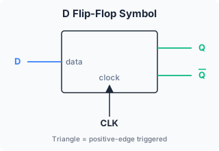
The triangle next to CLK denotes edge-triggered operation. If no bubble is present, the FF triggers on the rising edge. A bubble (circle) on the clock input indicates falling-edge triggering.
Modern Edge-Triggered Flip-Flops
The master-slave configuration is a pedagogical device: it explains how edge-triggered behaviour can be achieved from level-sensitive latches. Modern integrated circuits use truly edge-triggered designs that are more compact and have better timing characteristics, but their external behaviour is the same: D is sampled on the clock edge, and Q changes shortly afterwards.
For synchronous circuit design, the key abstraction is: the D flip-flop copies D to Q on the active clock edge, and Q holds that value until the next active edge. The characteristic equation is:
where Q’ is the state after the clock edge. This simple relationship is the foundation of all FSM design using D-FFs, covered in /modules/digital-electronics/08-synchronous-state-machines/02-fsm-design-procedure/.