Memories and ROMs
Read-Only Memory (ROM)
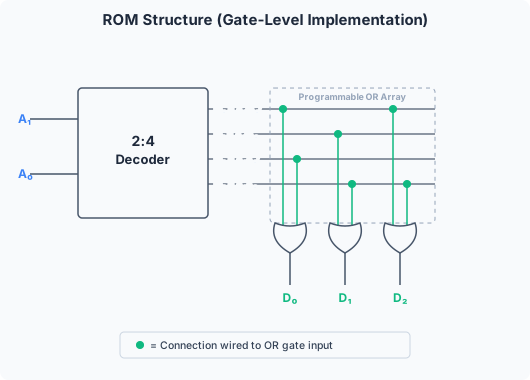
A ROM is a combinational circuit that implements a truth table as a permanent lookup table. It has n address inputs, m data outputs, and stores 2^n × m bits of data. For any address input, the corresponding stored word appears at the output.
The internal structure of a ROM mirrors the decoder-plus-OR-gates pattern: a decoder generates all minterms of the address, and an OR plane (or equivalent) connects the selected word to the outputs.
ROM as universal logic
Any n-input, m-output combinational function can be implemented with a 2^n × m ROM. No logic minimisation is needed: the truth table is simply “programmed” into the ROM by setting the storage bits appropriately. The delay is fixed (one ROM access time) regardless of function complexity.
Example: A 3-bit input, 2-bit output function f, g can be stored in an 8×2 ROM (3 address lines, 8 words of 2 bits each).
ROM types
| Type | Programmability | Erasable? | Notes |
|---|---|---|---|
| Mask ROM | At manufacture | No | Cheapest in volume, fixed content |
| PROM | Once by user | No | Fusible links, one-time programmable |
| EPROM | By user | UV light | Quartz window, ~20 min erase |
| EEPROM | By user | Electrically | Byte-erasable, slower write |
| Flash | By user | Electrically | Block erase, fast read, modern standard |
Flash memory is ubiquitous: BIOS/UEFI firmware, microcontroller program storage, SSDs, USB drives. Unlike SRAM, Flash is non-volatile — it retains data when power is removed. Unlike DRAM, it does not need periodic refresh.
SRAM (Static RAM)
SRAM uses a cross-coupled inverter pair (essentially two inverters in a feedback loop) to store each bit. This is a bistable circuit: it has two stable states (0 and 1). As long as power is applied, the bit is retained without refresh. This makes SRAM the simplest volatile memory.
SRAM is fast (access times ~1-10 ns), uses 6 transistors per cell (for CMOS SRAM), and is used for CPU caches, register files, and on-chip memories. It is volatile: removing power loses the data.
Memory capacity and expansion
A memory chip is characterised by its capacity: the number of addressable locations (words) and the width of each word.
For example, a 64K × 8 memory has 16 address lines (2^16 = 65536) and an 8-bit data bus, storing 64 KB total.
Word expansion (more addresses): multiple memory chips with a decoder selecting which chip is enabled for a given address range. The upper address bits feed the decoder; lower bits feed all chips.
Bit expansion (wider words): multiple memory chips connected in parallel, each handling a subset of the data bus bits. All chips share the same address and control signals.
Memory application
In the hardware labs, memory devices are used to store lookup tables and microprograms. The connection to programmable logic: a ROM can replace any combinational circuit, and a ROM-plus-register structure (a registered ROM) creates a simple sequential circuit — the register holds the current “state” and feeds back to the ROM’s address lines, effectively implementing an FSM.
Bus contention
When multiple memory or I/O devices share a data bus, only one may drive the bus at a time. Tristate buffers on the data outputs of each device ensure that only the device being read (selected by the address decoder) drives the bus; all others are in the high-impedance (Z) state. This is covered in detail in the tristate buffer note.