Field Programmable Gate Arrays (FPGA)
Why a different architecture
A GAL builds logic from a wide AND plane feeding a fixed OR plane. As you add inputs the AND plane size grows as , so the device stops scaling past a handful of feedback lines. A Field Programmable Gate Array (FPGA) takes a completely different approach: instead of one large programmable plane, it spreads many small programmable configurable logic blocks (CLBs) across a chip, surrounding them with a programmable routing network that wires the CLBs together and to the input/output blocks (IOBs) at the chip edge.
The key wins are:
- The CLBs are small and replicated, so the architecture scales with silicon density instead of hitting a structural wall.
- Routing between CLBs is programmable through switch matrices, so a large design can be partitioned across many CLBs and stitched together afterwards.
- Reprogramming happens by loading a configuration bitstream, which on some devices is stored in static RAM and can be replaced at power-up from an attached EEPROM.
FPGA architecture (Xilinx Spartan)
The course teaches the FPGA through the Xilinx Spartan family, because the parts are representative and well documented.
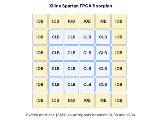
The IOBs at the edges provide the physical pins and input/output registers. The CLBs in the interior do the work. The routing between them is a network of wires and switch matrices (SMs) whose job is to connect any CLB output to any other CLB input, subject to routing congestion.
What is inside a Spartan CLB
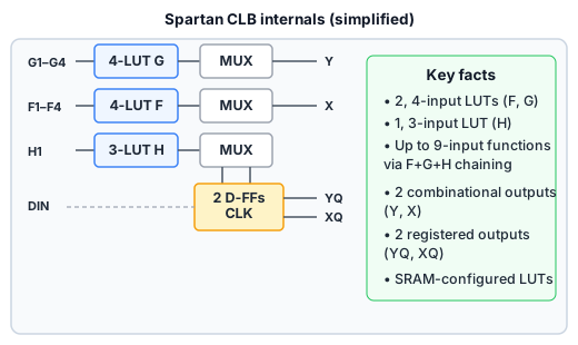
A Spartan CLB contains three look-up tables (LUTs), two D-type flip-flops and a set of multiplexers:
- Two 4-input LUTs, labelled F and G, each able to implement any 4-input Boolean function.
- One 3-input LUT, labelled H, which can combine the outputs of F and G (plus one external input) into a function of up to 9 inputs.
- Two outputs that bypass the flip-flops (Y, X), giving pure combinational results.
- Two registered outputs (YQ, XQ), which come from the D-FFs. Each D-FF can take its input from DIN, or from the F, G, or H LUT.
The multiplexers at the output of each LUT and at the D-FF inputs are what you configure: they decide which LUT feeds which output, and whether each output is registered or combinational. The LUTs themselves are programmed by writing their truth tables directly into small SRAM cells, which is why FPGAs can implement arbitrary combinational logic without a physical AND/OR plane.
Capacity of a single CLB
A single CLB can produce up to two combinational functions and two registered functions at the same time, because there are two outputs (X and Y) and two registers (XQ and YQ). All functions can involve at least four input variables (the F and G LUTs each take four), and some can be as wide as nine inputs by chaining F and G through the H LUT. State machines therefore fit nicely: the next-state logic goes into the LUTs and the state bits themselves are held in the D-FFs, exactly mirroring how you would build an FSM on paper.
Configuring the FPGA
The configuration information is the entire job of telling the chip what to do:
- the truth tables for every LUT in every CLB,
- the select signals for every multiplexer,
- the connections inside every switch matrix.
Xilinx Spartan parts store this configuration in static RAM (SRAM), which has two consequences. First, the configuration is volatile, so the chip loses its programming when power is removed. Second, the same chip can be reprogrammed in-circuit, which is ideal for development and for firmware updates in the field. At power-up the SRAM contents are typically loaded either from an attached EEPROM device or from a host computer over a JTAG-like interface. Parts from other manufacturers (Altera being the main alternative) follow the same idea but differ in cell structure, internal memory options and the size of the CLBs.
Other FPGA families and trade-offs
The Spartan is just one product line. Across manufacturers and families the differences you care about are:
- the number of CLBs on the chip, which sets how big a design fits;
- the structure of each CLB, in particular how many inputs each LUT accepts (4 vs 6 is the modern sweet spot);
- whether configuration is stored in internal non-volatile memory (some Actel parts) or external SRAM-backed (Xilinx, Altera);
- additional on-chip resources such as dedicated arithmetic blocks (multipliers, DSP slices), block RAM, clock management PLLs, and transceivers.
These extras do not change the basic story. They just make the FPGA better at the things designers actually want to do (signal processing, heavily pipelined datapaths, high-speed I/O), which is why FPGAs sit between GALs and full custom ASICs in the cost and flexibility spectrum.
Continue to the design flow that turns HDL into a configured FPGA:
See also: