Gate Propagation Delay
Physical reality of gates
Logic gates are not instantaneous. When an input changes, the output changes after a short but non-zero time called the propagation delay . This delay arises from the physical characteristics of transistors: charging and discharging capacitances in the transistors and wiring.
Two specific delays are often distinguished:
- : propagation delay for a Low-to-High output transition.
- : propagation delay for a High-to-Low output transition.
These may differ because the pull-up (p-MOS) and pull-down (n-MOS) transistors in CMOS have different drive strengths. For analysis we often use the worst case: .
Delay through a circuit
For a combinational circuit, the total propagation delay from any input to any output is the sum of the delays along the longest path (the critical path). Each gate contributes one (plus wire delay, which becomes significant at high speeds and is absorbed into the gate delay in this course).
Example: A 2-level SOP circuit (AND plane → OR plane) has critical path delay = .
Example: A 4-bit ripple carry adder has critical path = (for ) → (through carry chain). Specifically, the propagation from to passes through 4 full adders of carry logic.
Timing diagram conventions
Timing diagrams plot signal voltages against time.
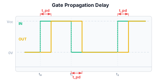
Key conventions:
- Transitions are drawn as sloping lines (ramps), not instantaneous steps, to indicate the finite switching time.
- Propagation delay is measured from the 50% point of the input transition to the 50% point of the output transition.
- Logic 1 and logic 0 are defined as voltage thresholds (e.g., > 3.5V = 1, < 1.5V = 0).
Rise time and fall time
The rise time is the time for a signal to transition from 10% to 90% of its final value (or 20% to 80% in some conventions). The fall time is the same for a high-to-low transition. Rise/fall times depend on the drive strength (current capability) of the output and the capacitive load being driven.
While rise/fall time calculations are not on the Tripos, the concept that signals take finite time to change is essential for understanding hazards and timing constraints.
Implications for circuit design
- Critical path analysis: The slowest path determines the maximum operating frequency. All other paths have “slack” — they could be slower without affecting overall performance.
- Glitches and hazards: Different path lengths through a circuit can cause transient incorrect outputs, as explored in the next note on hazards.
- Gate sizing: Larger transistors switch faster (more drive current) but consume more power and area. Critical path gates are often made larger; non-critical gates can be minimum size.
- Wire delay: At high speeds, the time for a signal to travel along a wire becomes comparable to gate delay. This is why FPGAs and ASICs include programmable routing delays in their timing models.