Simple Computer Architecture
The von Neumann architecture
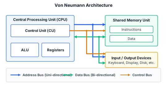
A modern digital computer, at its core, follows the von Neumann architecture, named after John von Neumann’s 1945 design. It has four main components:
- CPU (Central Processing Unit): The “brain” that executes instructions. Contains registers, an ALU, and a control unit.
- Memory (RAM): Stores both instructions (the program) and data. Instructions and data share the same memory space, connected to the CPU by buses.
- Address bus: Carries the memory address from the CPU to memory. The width of the address bus (in bits) determines the maximum addressable memory: N address lines can address 2^N locations.
- Data bus: Carries data between the CPU and memory. The width (e.g., 16-bit, 32-bit) determines how much data can be transferred in one operation.
The von Neumann architecture is a stored program computer: the program is stored in the same memory as data, and the CPU fetches, decodes, and executes instructions sequentially (unless a branch changes the flow). This is the basis of virtually every general-purpose computer, from microcontrollers to supercomputers.
CPU components
Registers: Small, fast storage locations inside the CPU (typically fewer than 100, may be as few as 4 in simple designs). Registers hold operands, intermediate results, and addresses. They are the fastest memory in the computer, operating at the CPU clock speed. The set of registers plus the Program Counter forms the architectural state of the processor.
ALU (Arithmetic Logic Unit): Performs arithmetic (add, subtract) and logical (AND, OR, NOT) operations on data from registers. The ALU’s operation is selected by control signals from the instruction decoder. It also produces flag outputs: a zero flag (set when the result is zero), a carry flag, a negative flag, etc. These flags are used by conditional branch instructions.
Instruction decoder and control unit: Interprets the current instruction’s opcode and generates all the control signals that orchestrate the datapath: which registers to read, what ALU operation to perform, whether to write to the register file or memory, which multiplexer selects to activate, and what the next program counter value should be.
Program Counter (PC): A special register that holds the memory address of the current instruction being fetched. After each fetch, the PC is normally incremented by one (to point to the next sequential instruction). Branches and jumps override this by loading a new address into the PC.
Architecture vs microarchitecture
This distinction is fundamental and examinable.
Architecture (or Instruction Set Architecture, ISA): The programmer-visible interface. It defines the instruction set, the set of registers, the memory addressing model, and the data types. For example, the MIPS architecture specifies 32 general-purpose registers (each 32 bits wide) and a fixed instruction set including ADD, SUB, LOAD, STORE, BEQ, etc. The architecture is the contract between hardware and software: any program written for the ISA will run on any microarchitecture that implements it.
Microarchitecture: The specific internal implementation of the architecture. It specifies how the datapath is organised, which components are used, how many ALUs, how the pipeline is arranged, how the control signals are generated. The same architecture can be implemented by many different microarchitectures, each with different cost/performance trade-offs. A single-cycle processor, a multicycle processor, and a pipelined processor can all implement the same ISA, but with vastly different performance and hardware complexity.
Example: the Intel x86 architecture has been implemented by hundreds of different microarchitectures over decades (Pentium, Core, etc.), all running the same x86 programs.
The instruction execution cycle
Every instruction follows the same fundamental cycle:
- Fetch: Read the instruction from memory at the address held in the PC. The instruction is loaded into the instruction register inside the CPU.
- Decode: The instruction decoder parses the instruction’s bit pattern to determine: the opcode (what operation to perform), the source register(s), the destination register, and any immediate values.
- Execute: Perform the operation. For an ADD, this means reading the source registers, running the ALU, and producing a result. For a LOAD, compute the memory address and read data memory.
- Writeback: Store the result back to the destination register (for R-type instructions) or to memory (for STORE).
After writeback, the PC advances (either to PC+1 for sequential execution, or to a branch target), and the cycle repeats.
MIPS example
In the MIPS architecture used as the running example in the course, the architectural state comprises:
- The Program Counter (PC), 32 bits wide.
- 32 general-purpose registers (R0 through R31), each 32 bits wide.
A simple instruction like ADD R1, R2, R3 means: register R1 ← register R2 + register R3. This involves reading two source registers, computing their sum in the ALU, and writing the result to the destination register, all in one instruction.
See /modules/digital-electronics/13-processor-architecture/02-microarchitecture-datapath-and-control/ for how the datapath and control unit are organised to implement this cycle.