Logic Families and Noise Margin
What is a logic family?
A logic family is a set of compatible integrated circuits (ICs) that share standardised electrical characteristics: voltage levels, timing, drive capability, and pin assignments. Gates within the same family can be connected directly without interface circuitry. Different families may have incompatible voltage thresholds, requiring level-shifting when mixed.
Voltage level specifications
Every logic family specifies four critical voltage thresholds:
| Symbol | Meaning |
|---|---|
| V_OH(min) | Minimum output voltage guaranteed for logic 1 |
| V_OL(max) | Maximum output voltage guaranteed for logic 0 |
| V_IH(min) | Minimum input voltage recognised as logic 1 |
| V_IL(max) | Maximum input voltage recognised as logic 0 |
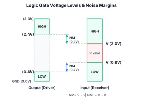
The gap between V_OL(max) and V_IL(max) (and between V_IH(min) and V_OH(min)) ensures that a gate’s output, when degraded by noise, still falls within the valid input ranges of the next gate.
Noise margin
The noise margin quantifies how much electrical noise a gate can tolerate on its inputs while still producing correct outputs. There are two noise margins:
Logic 0 noise margin: the maximum positive noise voltage that can be added to a logic 0 signal without the receiver misinterpreting it as undefined or logic 1:
Logic 1 noise margin: the maximum negative noise voltage that can be subtracted from a logic 1 signal without the receiver misinterpreting it:
The worst-case noise margin is min(NM_0, NM_1). A larger noise margin means the circuit is more robust.
Worked example: HCMOS (74HC)
The 74HC (High-Speed CMOS) family, used in the hardware labs, has the following specifications at V_DD = 5V (from the datasheet):
- V_OH(min) = 4.4V
- V_OL(max) = 0.1V
- V_IH(min) = 3.15V
- V_IL(max) = 1.35V
Noise margins:
The worst-case noise margin is 1.25V. This is excellent: nearly half the supply voltage range is noise margin. The undefined region (between V_IL(max) and V_IH(min)) is only 1.8V wide (from 1.35V to 3.15V).
Comparison with TTL
TTL (Transistor-Transistor Logic), the older 74 series standard:
| Property | TTL | HCMOS |
|---|---|---|
| Typical NM_0 | ~0.4V | 1.25V |
| Typical NM_1 | ~0.4V | 1.25V |
| Supply voltage | 5V ± 5% | 2-6V |
| Static power | Higher | Near zero |
| Input current | Significant | Negligible |
TTL has much lower noise margins (about 0.4V) because its output voltage levels are less close to the supply rails. TTL outputs swing between roughly 0.2V and 3.4V, whereas CMOS outputs swing nearly rail-to-rail (0V to V_DD). The narrow noise margins of TTL make it more susceptible to noise pickup from adjacent signals (crosstalk).
CMOS families
4000 series: The original CMOS family. Operates from 3V to 15V. Very slow by modern standards (gate delays ~60 ns). Robust but obsolete for high-speed designs.
74HC (High-Speed CMOS): Pin-compatible with 74-series TTL, providing a CMOS upgrade path. Gate delays ~10-20 ns. Wide supply range. The family used in the Cambridge hardware labs.
74HCT: Same as 74HC but with TTL-compatible input thresholds. V_IL(max) and V_IH(min) are shifted to match TTL levels, allowing direct interface between TTL outputs and CMOS inputs.
74AC (Advanced CMOS): Even faster, with gate delays around 3 ns.
Fan-out
Fan-out is the maximum number of gate inputs that a single gate output can reliably drive while maintaining valid voltage levels. It is determined by:
- DC fan-out: limited by the output current drive capability. A gate output can source or sink only so much current. In CMOS, inputs draw negligible DC current (they are capacitive), so DC fan-out is extremely high.
- AC fan-out: limited by input capacitance. Each gate input presents a capacitive load. Driving many inputs adds capacitance, slowing down transitions (RC time constant increases). The switching time becomes:
where N is the number of loads and C_input is the capacitance per input.
Transition time
The output transition time (rise time and fall time) depends on:
- Drive strength: the on-resistance of the output transistor. Lower resistance switches faster.
- Load capacitance: the sum of the input capacitances of the driven gates plus wiring capacitance.
- Supply voltage: higher V_DD means more drive current, giving faster switching (but more dynamic power).
In CMOS, the p-MOS transistor in the pull-up network is typically made wider than the n-MOS to compensate for the lower hole mobility, aiming for symmetric rise and fall times.
Tripos context
Noise margin calculations and logic family comparisons appear on the Tripos as short-answer parts of larger questions. You should know the definitions of all four voltage thresholds, be able to calculate both noise margins, and understand why CMOS has superior noise immunity compared to TTL. The 74HC numbers in the worked example above are the ones to memorise.
See /modules/digital-electronics/12-transistors-and-cmos-logic/02-nmos-inverter/ for the static power problem that noise margin specifications do not solve but that CMOS does.