CMOS Gates
General CMOS gate structure
Any CMOS logic gate follows the same architectural pattern:
- A pull-down network (PDN) made entirely of n-MOS transistors, connected between the output node and ground (0V). The PDN conducts (connects output to ground) when the logic function evaluates to TRUE, i.e., when the output should be LOW.
- A pull-up network (PUN) made entirely of p-MOS transistors, connected between V_DD and the output node. The PUN conducts (connects output to V_DD) when the logic function evaluates to FALSE, i.e., when the output should be HIGH.
The PDN and PUN are duals: they are never both ON at the same time. The PUN is the De Morgan complement of the PDN. Because p-MOS transistors turn ON when their gates are LOW, the PUN uses the same logic structure as the PDN but with complementary inputs.
The duality principle
- Series connection in the PDN becomes parallel in the PUN, and vice versa.
- The PDN implements the function F (pulls down when F is true); the PUN implements NOT(F) (pulls up when F is false).
- This follows from De Morgan’s theorem: if the PDN is (A · B), the PUN must be NOT(A · B) = NOT(A) + NOT(B). Since p-MOS turns on with a LOW gate, feeding it the same A and B signals effectively gives us NOT(A) + NOT(B) as wanted.
CMOS NAND gate
Function: Y = NOT(A · B). Output is LOW only when both A and B are HIGH.
- Pull-down network (PDN): Two n-MOS transistors in series. Both must be ON (A = 1 and B = 1) to connect V_out to ground.
- Pull-up network (PUN): Two p-MOS transistors in parallel. If either A = 0 or B = 0 (or both), at least one p-MOS is ON, connecting V_out to V_DD.
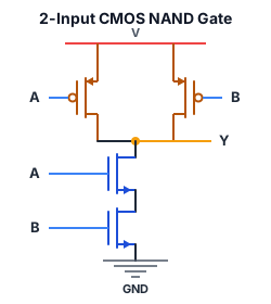
Truth table verification, assuming V_DD = 10V:
| A | B | T1 (n) | T2 (n) | T3 (p) | T4 (p) | V_out |
|---|---|---|---|---|---|---|
| 0 | 0 | OFF | OFF | ON | ON | 10V (1) |
| 0 | 1 | OFF | OFF | ON | ON | 10V (1) |
| 1 | 0 | OFF | OFF | ON | ON | 10V (1) |
| 1 | 1 | ON | ON | OFF | OFF | 0V (0) |
- T1, T2: n-MOS transistors in series (PDN). ON when gate = HIGH.
- T3, T4: p-MOS transistors in parallel (PUN). ON when gate = LOW.
A = 0, B = 0: T1 OFF, T2 OFF (series PDN is open). T3 ON (gate = 0), T4 ON (gate = 0), so V_out = V_DD = 1. A = 1, B = 1: T1 ON, T2 ON (series PDN connects V_out to ground). T3 OFF (gate = 10V), T4 OFF (gate = 10V), so V_out = 0.
CMOS NOR gate
Function: Y = NOT(A + B). Output is HIGH only when both A and B are LOW.
- Pull-down network (PDN): Two n-MOS transistors in parallel. If either A = 1 or B = 1, V_out is pulled to ground.
- Pull-up network (PUN): Two p-MOS transistors in series. Both must be ON (A = 0 and B = 0) to connect V_out to V_DD.
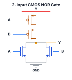
Truth table verification:
| A | B | T1 (n) | T2 (n) | T3 (p) | T4 (p) | V_out |
|---|---|---|---|---|---|---|
| 0 | 0 | OFF | OFF | ON | ON | 10V (1) |
| 0 | 1 | OFF | ON | ON | OFF | 0V (0) |
| 1 | 0 | ON | OFF | OFF | ON | 0V (0) |
| 1 | 1 | ON | ON | OFF | OFF | 0V (0) |
- T1, T2: n-MOS in parallel (PDN). Either or both ON pulls output LOW.
- T3, T4: p-MOS in series (PUN). Both must be ON to pull output HIGH.
The duality pattern
| PDN (n-MOS) | PUN (p-MOS) | Gate function |
|---|---|---|
| Single transistor | Single transistor | Inverter (NOT) |
| Series (AND form) | Parallel | NAND |
| Parallel (OR form) | Series | NOR |
More complex functions (AND-OR-INVERT, OR-AND-INVERT) follow the same principle. Any Boolean expression can be implemented as a CMOS gate if it can be expressed in a form where the PDN is a series-parallel network of n-MOS transistors.
Key points for the Tripos
- You must be able to draw the transistor-level schematic for a CMOS NAND or NOR gate given the gate-level symbol, and vice versa: identify the gate function from a transistor schematic.
- You must be able to verify the truth table by tracing which transistors are ON and OFF for each input combination.
- The rule for determining transistor state:
- n-MOS: ON when gate is HIGH (more positive than source, which is at ground, so gate = 1).
- p-MOS: ON when gate is LOW (more negative than source, which is at V_DD, so gate = 0).
- The PUN and PDN are duals: series becomes parallel and vice versa.
For the n-MOS inverter that this family replaces, see /modules/digital-electronics/12-transistors-and-cmos-logic/02-nmos-inverter/. For the broader context of how these gates fit into standardised logic families, see /modules/digital-electronics/12-transistors-and-cmos-logic/05-logic-families-and-noise-margin/.