The CMOS Inverter
The problem with n-MOS
The n-MOS inverter (see /modules/digital-electronics/12-transistors-and-cmos-logic/02-nmos-inverter/) has two fatal flaws:
- Static power dissipation: when the transistor is ON, current flows continuously through the pull-up resistor.
- Slow rise time: the output charges through the high-value pull-up resistor, giving a large RC time constant.
Circuit structure
The CMOS (Complementary MOS) inverter uses one n-MOS and one p-MOS transistor:
- n-MOS: source connected to ground (0V), drain connected to V_out, gate connected to V_in.
- p-MOS: source connected to V_DD, drain connected to V_out, gate connected to V_in.
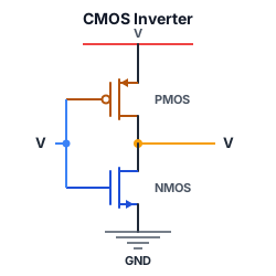
The two gates are tied together as the input. The two drains are tied together as the output.
Operation
Case 1: V_in = 0V (logic 0)
- n-MOS: V_GS = 0V < V_T → OFF (open circuit from V_out to ground).
- p-MOS: V_GS = -V_DD (gate is at 0V, source is at V_DD, so gate is negative relative to source) → ON (low-resistance path from V_DD to V_out).
- V_out = V_DD through the p-MOS. Strong logic 1.
Case 2: V_in = V_DD (logic 1)
- n-MOS: V_GS = V_DD > V_T → ON (low-resistance path from V_out to ground).
- p-MOS: V_GS = 0V (gate and source both at V_DD) → OFF (open circuit from V_DD to V_out).
- V_out = 0V through the n-MOS. Strong logic 0.
The two transistors are never both ON at the same time during steady state. One is always OFF, completely blocking any current path from V_DD to ground.
The critical advantage: near-zero static power
In either stable state (V_in = 0 or V_in = V_DD), one transistor is OFF and the other is ON. The OFF transistor is essentially an open circuit, so no DC current flows from V_DD to ground. The static power dissipation is effectively zero (only leakage currents, which are nanoamps in modern devices).
Power is only dissipated during switching, when both transistors are briefly ON simultaneously and current flows from V_DD to ground while the output capacitance charges or discharges. This dynamic power is proportional to the switching frequency, the square of the supply voltage, and the load capacitance:
This is still significant in high-speed chips, but it scales with activity: gates that are not switching consume negligible power.
Symmetrical switching
Unlike the n-MOS inverter, the CMOS inverter has symmetrical drive capability:
- Rising edge: the p-MOS transistor turns ON and actively pulls the output HIGH through a low-resistance path. The output capacitance charges quickly.
- Falling edge: the n-MOS transistor turns ON and actively pulls the output LOW through a low-resistance path. The output capacitance discharges quickly.
Both edges are fast. The transistor sizes are typically chosen so that the p-MOS and n-MOS have comparable on-resistances (p-MOS is usually made wider to compensate for the lower hole mobility).
Transfer characteristic
Plot V_out against V_in:
- When V_in is low (< V_Tn), the n-MOS is OFF and the p-MOS is ON. V_out = V_DD.
- As V_in increases past V_Tn, the n-MOS begins to turn on while the p-MOS is still on. Both conduct, V_out begins to fall.
- Near V_DD/2, both transistors are conducting significantly: this is the high-gain transition region.
- As V_in approaches (V_DD - |V_Tp|), the p-MOS turns off. V_out ≈ 0V.
- When V_in is high, the n-MOS is ON and p-MOS is OFF. V_out = 0V.
The switching threshold is around V_DD/2 for a well-designed inverter, giving balanced noise margins (see /modules/digital-electronics/12-transistors-and-cmos-logic/05-logic-families-and-noise-margin/).
Summary: n-MOS vs CMOS
| Property | n-MOS inverter | CMOS inverter |
|---|---|---|
| Pull-up | Resistor | p-MOS transistor |
| Pull-down | n-MOS | n-MOS |
| Static power | High (when output LOW) | Near zero |
| Output HIGH strength | Weak (through resistor) | Strong (through p-MOS) |
| Output LOW strength | Strong (through n-MOS) | Strong (through n-MOS) |
| Rise time | Slow (RC through resistor) | Fast (through p-MOS) |
| Fall time | Fast (through n-MOS) | Fast (through n-MOS) |
This is why CMOS has been the dominant logic family since the 1980s. The CMOS inverter is the fundamental building block from which all other CMOS gates are constructed (see /modules/digital-electronics/12-transistors-and-cmos-logic/04-cmos-gates/).