The n-MOS Inverter
Circuit structure
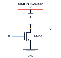
The simplest MOS logic gate: an n-MOS transistor with a passive pull-up resistor. The circuit:
- A resistor R₁ connects V_DD (supply voltage, e.g., 10V) to the output node V_out.
- An n-MOS transistor connects V_out to ground (0V). Its source is at ground, drain at V_out.
- The input voltage V_in is applied to the gate of the transistor.
Operation
Case 1: V_in = 0V (logic 0)
The gate voltage V_GS = 0V, which is below the threshold V_T. The transistor is OFF (open circuit). No current flows through R₁. By Ohm’s Law, the voltage drop across R₁ is zero, so V_out = V_DD = 10V. This is logic 1. The inverter works: input LOW → output HIGH.
Case 2: V_in = V_DD = 10V (logic 1)
Now V_GS = 10V, well above V_T. The transistor is ON. Current flows from V_DD through R₁, then through the transistor to ground. The transistor has some finite on-resistance R_DS(on). The circuit becomes a potential divider:
Since R_DS(on) is small compared to R₁ (ideally near zero), V_out is close to 0V. The inverter works: input HIGH → output LOW.
Graphical load-line analysis
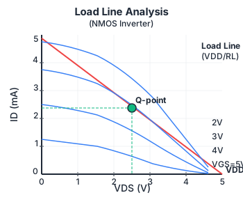
The n-MOS inverter is analysed graphically because the transistor is a nonlinear device with I-V curves that depend on V_GS. The method (from the slides with V_DD = 10V, R₁ = 1 kΩ):
-
The load line: This is the I-V characteristic of the resistor R₁, plotted on the axes of transistor V_DS (which is V_out) vs I_DS (which is the current through both the resistor and transistor). By KVL: V_DD = I_DS × R₁ + V_DS. Rearranging: I_DS = (V_DD - V_DS)/R₁. This is a straight line with intercepts at V_DS = 0, I_DS = V_DD/R₁ = 10/1000 = 10 mA, and V_DS = V_DD, I_DS = 0.
-
Transistor curves: For each value of V_GS (= V_in), the transistor has a specific I-V curve relating I_DS to V_DS. The course slides provide these curves (Fig. 1(b) in Examples Paper 3, Question 6).
-
Intersection: The operating point (V_out, I_DS) is where the load line intersects the transistor curve for the given V_GS. This is because the same current must flow through both the resistor and the transistor (they are in series), and KVL must be satisfied.
For V_in = 0V: The transistor curve is essentially a horizontal line at I_DS = 0 (transistor off). The load line at I_DS = 0 gives V_DS = V_DD = 10V. So V_out = 10V.
For V_in = 10V: The transistor is fully on. The intersection of the V_GS = 10V curve with the load line gives, from the example in the slides, V_out ≈ 1V and I_DS ≈ 9 mA.
Power dissipation: the fundamental problem
Transistor OFF (V_in = 0): I = 0, so P = IV = 0. No power dissipated in R₁, no power dissipated in the transistor. This is fine.
Transistor ON (V_in = 10V, V_out ≈ 1V): Current flows continuously.
Voltage across R₁: V_R1 = V_DD - V_out = 10 - 1 = 9V. Current through both: I = V_R1 / R₁ = 9/1000 = 9 mA.
Power in the resistor:
Power in the transistor:
Total static power: 81 + 9 = 90 mW per gate. In a chip with millions of gates, half of which might be on at any time, this static power consumption is catastrophic. This is not a problem of bad design: it is inherent to the n-MOS inverter architecture. Whenever the output is LOW, current flows from V_DD through the pull-up resistor to ground.
The rise-time problem
When the transistor turns OFF, the output must rise from ~0V to V_DD. There is always some stray capacitance C on the output node (from wiring, from the input of the next gate). This capacitor must charge through the pull-up resistor R₁. The RC time constant τ = R₁ × C determines the rise time. Since R₁ is typically large (to limit static power), the rise time is slow.
When the transistor turns ON, C discharges through the transistor’s low on-resistance R_DS(on), so the fall time is much faster. The n-MOS inverter has asymmetric switching times: slow rising edge, fast falling edge.
Both the static power problem and the asymmetric switching problem were solved by CMOS (Complementary MOS) logic (see /modules/digital-electronics/12-transistors-and-cmos-logic/03-cmos-inverter/).
Tripos exam context
Question 6 of Examples Paper 3 is a classic exam-style question:
The n-MOS FET with the characteristics shown in Fig. 1(b) is used to implement the inverter circuit shown in Fig. 1(a). (a) Draw a load line on Fig. 1(b) and determine V_out for V_in = 0V and 10V. (b) Calculate the power dissipated in the resistor and transistor for each input voltage.
You need to be able to: draw the load line, read off the intersection point from the transistor characteristic curves, and calculate the power in both components. This appears in Tripos Q2-2012 and Q2-2015.