The p-n Junction and Diodes
The p-n junction at equilibrium
When p-type and n-type silicon are brought together to form a junction, a remarkable thing happens without any external voltage applied.
Diffusion: There is a huge concentration gradient at the junction. The n-side has many free electrons, the p-side has many free holes. Carriers diffuse across the junction: electrons from the n-side move into the p-side, and holes from the p-side move into the n-side.
Depletion region: When an electron leaves the n-side, it leaves behind an immobile positive donor ion. When a hole leaves the p-side, it leaves behind an immobile negative acceptor ion. Near the junction, these exposed ions create a space-charge region (also called the depletion region) where there are essentially no free charge carriers. The positive ions on the n-side and negative ions on the p-side set up a built-in electric field pointing from the n-side to the p-side.
Equilibrium: The built-in field opposes further diffusion. Electrons trying to cross from n to p are pushed back by the field. A dynamic equilibrium is reached: the diffusion current (carriers moving down the concentration gradient) is balanced by the drift current (carriers moving under the influence of the electric field). No net current flows.
Forward bias
Connect the positive terminal of a battery to the p-side (anode) and the negative terminal to the n-side (cathode).
The external voltage reduces the potential barrier at the junction. Holes on the p-side are pushed toward the junction, electrons on the n-side are pushed toward the junction. They meet and neutralise some of the space charge, narrowing the depletion region and reducing the built-in field.
With a reduced opposing field, diffusion current dominates. Significant current flows. Increasing the forward bias voltage increases the current exponentially:
where I_S is the reverse saturation current (very small, typically nA), V_D is the forward voltage, and V_T is the thermal voltage (about 26 mV at room temperature). For typical silicon diodes, a forward bias of about 0.6-0.7V is needed to get significant current (the “knee” voltage).
Reverse bias
Connect the positive terminal to the n-side and the negative terminal to the p-side.
The external voltage reinforces the built-in field. Electrons are pulled out of the p-side, holes are pulled out of the n-side, widening the depletion region and increasing the barrier. Diffusion is suppressed even further. Only a tiny reverse saturation current I_S flows (of order nanoamps), carried by minority carriers (the few holes in the n-side and few electrons in the p-side) that are swept across the junction by the strong field.
For digital circuit purposes: reverse bias = no current flows. The junction is “off”.
At very high reverse voltages, breakdown occurs (Zener breakdown or avalanche breakdown). This is destructive in normal diodes but deliberately used in Zener diodes for voltage regulation.
The diode as a circuit element
A diode is a two-terminal device consisting of a single p-n junction. The terminal connected to the p-side is the anode; the terminal connected to the n-side is the cathode. The diode conducts current only when the anode is more positive than the cathode (forward biased).
The circuit symbol has an arrow pointing from anode to cathode, indicating the direction of conventional current flow under forward bias:
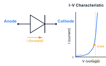
The diode is a one-way valve for current. In the ideal model: zero resistance when forward biased, infinite resistance when reverse biased.
Diodes in digital circuits
Digital circuits use diodes for:
- ESD (Electrostatic Discharge) protection: Diodes connected from each input pin to V_DD and ground clamp any voltage spikes that could damage the sensitive gate oxide of MOSFETs.
- Input protection: Logic gate inputs often have diode networks to prevent input voltages from exceeding the supply rails.
p-n junctions inside MOSFETs
The MOSFET itself contains p-n junctions. In an n-channel MOSFET (see /modules/digital-electronics/12-transistors-and-cmos-logic/01-mosfet-operation/), the source and drain are n-type regions in a p-type substrate. The source-substrate and drain-substrate boundaries are p-n junctions. These junctions are always kept reverse-biased in normal operation to prevent current from flowing between the source/drain and the substrate. The gate is insulated from the channel by silicon dioxide, so no DC gate current flows: the MOSFET is a voltage-controlled device, not a current-controlled one.
The diode’s role in the Tripos is a supporting one. You need to understand the p-n junction conceptually, recognise the diode as a one-way valve, and know that MOSFETs contain p-n junctions at their source and drain terminals. The detailed I-V equation is less important than the qualitative behaviour.