Potential Dividers
The potential divider formula
A potential (voltage) divider is simply two resistors in series across a voltage source. The voltage at the midpoint is a fraction of the supply voltage, determined by the resistor ratio. This is one of the most important sub-circuits in all of electronics.
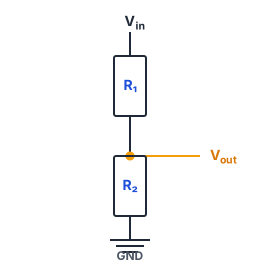
Consider a voltage V applied across R₁ and R₂ in series. The same current I flows through both:
The voltage across R₂ (the output, measured at the midpoint relative to ground) is:
More generally, for any resistor R_k in a chain of N resistors in series:
Worked examples
Example 1: V = 10V, R₁ = 1 kΩ, R₂ = 2 kΩ.
Example 2: V = 5V, R₁ = 10 kΩ, R₂ = 10 kΩ.
Equal resistors produce exactly half the supply voltage.
Example 3: A potentiometer (variable resistor) with total resistance 10 kΩ, wiper at 70% from ground. V = 5V.
Applications
Setting reference voltages: A potential divider can produce any voltage between 0 and V, used to set comparator thresholds or bias voltages for transistors.
Bias for transistor circuits: In the n-MOS inverter /modules/digital-electronics/12-transistors-and-cmos-logic/02-nmos-inverter/, the resistor and transistor form a nonlinear potential divider: when the transistor is on, V_out is determined by the ratio of its on-resistance to the pull-up resistor.
Sensors: A resistive sensor (thermistor, LDR) can be placed as one leg of a divider to convert a resistance change into a measurable voltage change.
Loaded vs unloaded voltage divider
The formula V × R₂/(R₁ + R₂) assumes no current is drawn from the midpoint (the output is unloaded). When a load resistance R_L is connected from the midpoint to ground, it draws current and the output voltage drops.
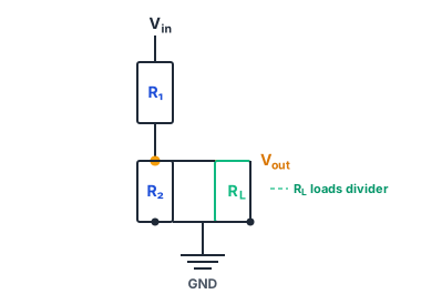
The load is in parallel with R₂, so the effective lower resistance becomes:
The output voltage under load is then:
Worked example: V = 6V, R₁ = 1 kΩ, R₂ = 1 kΩ, R_L = 1 kΩ.
Unloaded: V_out = 6 × 1/(1 + 1) = 3V.
Loaded: R_{2,eff} = (1 × 1)/(1 + 1) = 0.5 kΩ = 500 Ω.
The output drops from 3V to 2V: the load “pulls down” the divider. The heavier the load (lower R_L), the more severe the drop. This is why potential dividers used for reference voltages must have their values chosen so that the load current is negligible compared to the divider current.
Connection to Thévenin’s theorem
Any linear circuit can be reduced to an equivalent circuit consisting of a single voltage source V_th in series with a single resistance R_th. For the potential divider:
The Thévenin voltage V_th is the open-circuit output voltage:
The Thévenin resistance R_th is the resistance seen looking back into the output terminals with the voltage source replaced by a short circuit. This gives R₁ and R₂ in parallel:
The loaded divider analysis above is equivalent to asking: what is the voltage across R_L when driven by the Thévenin equivalent? Using the voltage divider formula on the Thévenin circuit:
For our example: V_th = 3V, R_th = 500 Ω, R_L = 1000 Ω.
Same result. Thévenin’s theorem is a preview of a technique used extensively in the n-MOS inverter analysis /modules/digital-electronics/12-transistors-and-cmos-logic/02-nmos-inverter/, where the pull-up resistor and supply are replaced by their Thévenin equivalent to help analyse the nonlinear transistor behaviour.
Graphical approach
The potential divider can also be solved graphically. Plot the I-V characteristic of R₂ (a straight line through the origin with slope 1/R₂). Plot the I-V characteristic of R₁, but reflected in terms of V₂ = V - V₁. Where the two curves intersect gives the operating point: the current is equal through both resistors, and V₂ is the voltage across R₂.
This graphical approach generalises to nonlinear devices: replace the R₂ characteristic with the I-V curve of a transistor, for example, and the intersection with the load line (R₁ characteristic) gives the operating point. This is exactly how the n-MOS inverter is analysed (see the graphical load-line analysis in /modules/digital-electronics/12-transistors-and-cmos-logic/02-nmos-inverter/).